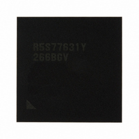
R5S77631Y266BGV Renesas Electronics America, R5S77631Y266BGV Datasheet - Page 470

R5S77631Y266BGV
Manufacturer Part Number
R5S77631Y266BGV
Description
IC SUPERH MPU ROMLESS 499BGA
Manufacturer
Renesas Electronics America
Series
SuperH® SH7780r
Datasheet
1.R5S77631Y266BGV.pdf
(2056 pages)
Specifications of R5S77631Y266BGV
Core Processor
SH-4A
Core Size
32-Bit
Speed
266MHz
Connectivity
Audio Codec, I²C, MMC, SCI, SIM, SIO, SSI, USB
Peripherals
DMA, LCD, POR, WDT
Number Of I /o
107
Program Memory Type
ROMless
Ram Size
16K x 8
Voltage - Supply (vcc/vdd)
1.15 V ~ 1.35 V
Data Converters
A/D 4x10b; D/A 2x8b
Oscillator Type
External
Operating Temperature
-20°C ~ 75°C
Package / Case
499-BGA
Lead Free Status / RoHS Status
Lead free / RoHS Compliant
Eeprom Size
-
Program Memory Size
-
Available stocks
Company
Part Number
Manufacturer
Quantity
Price
Company:
Part Number:
R5S77631Y266BGV
Manufacturer:
Renesas Electronics America
Quantity:
10 000
- Current page: 470 of 2056
- Download datasheet (10Mb)
Section 11 Local Bus State Controller (LBSC)
11.5.7
The byte control SRAM interface is a memory interface that outputs a byte-select strobe (WEn) in
both read and write bus cycles. This interface has 16-bit data pins and can be connected to SRAM
having an upper byte select strobe and lower select strobe functions, such as UB and LB.
Areas 1 and 4 can be specified as a byte control SRAM interface. However, when these areas are
set to the MPX interface, the MPX interface has priority.
The write timing for the byte control SRAM interface is identical to that of a normal SRAM
interface.
In read operations, on the other hand, the WEn pin timing is different. In a read access, only the
WE signal for the byte being read is asserted. Assertion is synchronized with the falling edge of
the CLKOUT clock in the same way as for the WE signal, while negation is synchronized with the
rising edge of the CLKOUT clock in the same way as for the RD signal.
In 32-byte transfer, a total of 32 bytes are transferred continuously according to the set bus width.
The first access is performed on the data for which there was an access request, and the remaining
accesses are performed in wrap around method according to the set bus width. The bus is not
released during this transfer.
Figure 11.35 shows an example of a byte control SRAM connection, and figures 11.36 to 11.38
show examples of byte-control SRAM read cycles.
Rev. 2.00 May 22, 2009 Page 400 of 1982
REJ09B0256-0200
Byte Control SRAM Interface
Figure 11.35 Example of 32-Bit Data-Width Byte-Control SRAM
This LSI
D31 to D16
D15 to D0
A18 to A3
RDWR
WE3
WE2
WE1
WE0
CSn
RD
A15 to A0
CS
OE
WE
I/O15 to I/O0
UB
LB
A15 to A0
CS
OE
WE
I/O15 to I/O0
UB
LB
64K × 16-bit
SRAM
Related parts for R5S77631Y266BGV
Image
Part Number
Description
Manufacturer
Datasheet
Request
R

Part Number:
Description:
KIT STARTER FOR M16C/29
Manufacturer:
Renesas Electronics America
Datasheet:

Part Number:
Description:
KIT STARTER FOR R8C/2D
Manufacturer:
Renesas Electronics America
Datasheet:

Part Number:
Description:
R0K33062P STARTER KIT
Manufacturer:
Renesas Electronics America
Datasheet:

Part Number:
Description:
KIT STARTER FOR R8C/23 E8A
Manufacturer:
Renesas Electronics America
Datasheet:

Part Number:
Description:
KIT STARTER FOR R8C/25
Manufacturer:
Renesas Electronics America
Datasheet:

Part Number:
Description:
KIT STARTER H8S2456 SHARPE DSPLY
Manufacturer:
Renesas Electronics America
Datasheet:

Part Number:
Description:
KIT STARTER FOR R8C38C
Manufacturer:
Renesas Electronics America
Datasheet:

Part Number:
Description:
KIT STARTER FOR R8C35C
Manufacturer:
Renesas Electronics America
Datasheet:

Part Number:
Description:
KIT STARTER FOR R8CL3AC+LCD APPS
Manufacturer:
Renesas Electronics America
Datasheet:

Part Number:
Description:
KIT STARTER FOR RX610
Manufacturer:
Renesas Electronics America
Datasheet:

Part Number:
Description:
KIT STARTER FOR R32C/118
Manufacturer:
Renesas Electronics America
Datasheet:

Part Number:
Description:
KIT DEV RSK-R8C/26-29
Manufacturer:
Renesas Electronics America
Datasheet:

Part Number:
Description:
KIT STARTER FOR SH7124
Manufacturer:
Renesas Electronics America
Datasheet:

Part Number:
Description:
KIT STARTER FOR H8SX/1622
Manufacturer:
Renesas Electronics America
Datasheet:

Part Number:
Description:
KIT DEV FOR SH7203
Manufacturer:
Renesas Electronics America
Datasheet:


