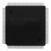
HD6417032F20V Renesas Electronics America, HD6417032F20V Datasheet - Page 31

HD6417032F20V
Manufacturer Part Number
HD6417032F20V
Description
SH1 ROMLESS LEAD FREE
Manufacturer
Renesas Electronics America
Series
SuperH® SH7030r
Datasheet
1.HD6417034AFI20.pdf
(689 pages)
Specifications of HD6417032F20V
Core Processor
SH-1
Core Size
32-Bit
Speed
20MHz
Connectivity
EBI/EMI, SCI
Peripherals
DMA, POR, PWM, WDT
Number Of I /o
32
Program Memory Type
ROMless
Ram Size
4K x 8
Voltage - Supply (vcc/vdd)
4.5 V ~ 5.5 V
Data Converters
A/D 8x10b
Oscillator Type
Internal
Operating Temperature
-20°C ~ 75°C
Package / Case
112-QFP
Lead Free Status / RoHS Status
Lead free / RoHS Compliant
Eeprom Size
-
Program Memory Size
-
Available stocks
Company
Part Number
Manufacturer
Quantity
Price
Company:
Part Number:
HD6417032F20V
Manufacturer:
TI
Quantity:
201
- Current page: 31 of 689
- Download datasheet (5Mb)
Feature
Interrupt controller
(INTC)
User break controller
(UBC)
Clock pulse generator
(CPG)
Bus state controller
(BSC)
Description
Nine external interrupt pins (NMI, IRQ0–IRQ7)
Thirty-one internal interrupt sources
Sixteen programmable priority levels
Generates an interrupt when the CPU or DMAC generates a bus cycle
with specified conditions
Simplifies configuration of an on-chip debugger
On-chip clock pulse generator (maximum operating frequency: 20 MHz):
20-MHz pulses can be generated from a 20-MHz crystal with a duty cycle
Supports external memory access:
Sixteen-bit external data bus
Address space divided into eight areas with the following preset features:
Bus size (8 or 16 bits)
Number of wait cycles can be defined by user.
Type of area (external memory area, DRAM area, etc.)
When the DRAM area is accessed:
Chip select signals (CS0 to CS7) are output for each area
DRAM refresh function:
Programmable refresh interval
Supports CAS-before-RAS refresh and self-refresh modes
DRAM burst access function:
Supports high-speed access modes for DRAM
Wait cycles can be inserted by an external WAIT signal
One-stage write buffer improves the system performance
Data bus parity can be generated and checked
correcting circuit
Simplifies connection to ROM, SRAM, DRAM, and peripheral I/O
RAS and CAS signals for DRAM are output
Tp cycles can be generated to assure RAS precharge time
Address multiplexing is supported internally, so DRAM can be
connected directly
Rev. 7.00 Jan 31, 2006 page 3 of 658
Section 1 Overview
REJ09B0272-0700
Related parts for HD6417032F20V
Image
Part Number
Description
Manufacturer
Datasheet
Request
R

Part Number:
Description:
KIT STARTER FOR M16C/29
Manufacturer:
Renesas Electronics America
Datasheet:

Part Number:
Description:
KIT STARTER FOR R8C/2D
Manufacturer:
Renesas Electronics America
Datasheet:

Part Number:
Description:
R0K33062P STARTER KIT
Manufacturer:
Renesas Electronics America
Datasheet:

Part Number:
Description:
KIT STARTER FOR R8C/23 E8A
Manufacturer:
Renesas Electronics America
Datasheet:

Part Number:
Description:
KIT STARTER FOR R8C/25
Manufacturer:
Renesas Electronics America
Datasheet:

Part Number:
Description:
KIT STARTER H8S2456 SHARPE DSPLY
Manufacturer:
Renesas Electronics America
Datasheet:

Part Number:
Description:
KIT STARTER FOR R8C38C
Manufacturer:
Renesas Electronics America
Datasheet:

Part Number:
Description:
KIT STARTER FOR R8C35C
Manufacturer:
Renesas Electronics America
Datasheet:

Part Number:
Description:
KIT STARTER FOR R8CL3AC+LCD APPS
Manufacturer:
Renesas Electronics America
Datasheet:

Part Number:
Description:
KIT STARTER FOR RX610
Manufacturer:
Renesas Electronics America
Datasheet:

Part Number:
Description:
KIT STARTER FOR R32C/118
Manufacturer:
Renesas Electronics America
Datasheet:

Part Number:
Description:
KIT DEV RSK-R8C/26-29
Manufacturer:
Renesas Electronics America
Datasheet:

Part Number:
Description:
KIT STARTER FOR SH7124
Manufacturer:
Renesas Electronics America
Datasheet:

Part Number:
Description:
KIT STARTER FOR H8SX/1622
Manufacturer:
Renesas Electronics America
Datasheet:

Part Number:
Description:
KIT DEV FOR SH7203
Manufacturer:
Renesas Electronics America
Datasheet:


