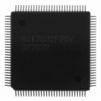
HD6417032F20V Renesas Electronics America, HD6417032F20V Datasheet - Page 179

HD6417032F20V
Manufacturer Part Number
HD6417032F20V
Description
SH1 ROMLESS LEAD FREE
Manufacturer
Renesas Electronics America
Series
SuperH® SH7030r
Datasheet
1.HD6417034AFI20.pdf
(689 pages)
Specifications of HD6417032F20V
Core Processor
SH-1
Core Size
32-Bit
Speed
20MHz
Connectivity
EBI/EMI, SCI
Peripherals
DMA, POR, PWM, WDT
Number Of I /o
32
Program Memory Type
ROMless
Ram Size
4K x 8
Voltage - Supply (vcc/vdd)
4.5 V ~ 5.5 V
Data Converters
A/D 8x10b
Oscillator Type
Internal
Operating Temperature
-20°C ~ 75°C
Package / Case
112-QFP
Lead Free Status / RoHS Status
Lead free / RoHS Compliant
Eeprom Size
-
Program Memory Size
-
Available stocks
Company
Part Number
Manufacturer
Quantity
Price
Company:
Part Number:
HD6417032F20V
Manufacturer:
TI
Quantity:
201
- Current page: 179 of 689
- Download datasheet (5Mb)
Section 8 Bus State Controller (BSC)
Regardless of the state of the WAIT signal, when the RW1 bit, the number of wait states selected
by CBR refresh wait state insertion bits 1 and 0 (RLW1, RLW0) in the refresh control register
(RCR) are inserted into the CAS-before-RAS refresh cycle.
8.5.4
Byte Access Control
16-bit width and 18-bit width DRAMs require different types of byte control signals for access. By
setting the dual CAS signals/dual WE signals select bit (CW2) in DCR, the BSC allows selection
of either the dual CAS signal or dual WE signal system of control signals. When 16-bit space is
being accessed and the CW2 bit is cleared to 0 for dual CAS signals, CASH, CASL, and WRL
signals are output; when CW2 is set to 1 for dual WE signals, the CASL, WRH, and WRL signals
are output. When accessing 8-bit space, WRL and CASL are output regardless of the CW2 setting.
Figure 8.21 shows the control timing of the upper byte write cycle (short pitch) in 16-bit space.
Rev. 7.00 Jan 31, 2006 page 151 of 658
REJ09B0272-0700
Related parts for HD6417032F20V
Image
Part Number
Description
Manufacturer
Datasheet
Request
R

Part Number:
Description:
KIT STARTER FOR M16C/29
Manufacturer:
Renesas Electronics America
Datasheet:

Part Number:
Description:
KIT STARTER FOR R8C/2D
Manufacturer:
Renesas Electronics America
Datasheet:

Part Number:
Description:
R0K33062P STARTER KIT
Manufacturer:
Renesas Electronics America
Datasheet:

Part Number:
Description:
KIT STARTER FOR R8C/23 E8A
Manufacturer:
Renesas Electronics America
Datasheet:

Part Number:
Description:
KIT STARTER FOR R8C/25
Manufacturer:
Renesas Electronics America
Datasheet:

Part Number:
Description:
KIT STARTER H8S2456 SHARPE DSPLY
Manufacturer:
Renesas Electronics America
Datasheet:

Part Number:
Description:
KIT STARTER FOR R8C38C
Manufacturer:
Renesas Electronics America
Datasheet:

Part Number:
Description:
KIT STARTER FOR R8C35C
Manufacturer:
Renesas Electronics America
Datasheet:

Part Number:
Description:
KIT STARTER FOR R8CL3AC+LCD APPS
Manufacturer:
Renesas Electronics America
Datasheet:

Part Number:
Description:
KIT STARTER FOR RX610
Manufacturer:
Renesas Electronics America
Datasheet:

Part Number:
Description:
KIT STARTER FOR R32C/118
Manufacturer:
Renesas Electronics America
Datasheet:

Part Number:
Description:
KIT DEV RSK-R8C/26-29
Manufacturer:
Renesas Electronics America
Datasheet:

Part Number:
Description:
KIT STARTER FOR SH7124
Manufacturer:
Renesas Electronics America
Datasheet:

Part Number:
Description:
KIT STARTER FOR H8SX/1622
Manufacturer:
Renesas Electronics America
Datasheet:

Part Number:
Description:
KIT DEV FOR SH7203
Manufacturer:
Renesas Electronics America
Datasheet:


