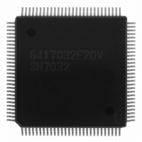
HD6417032F20V Renesas Electronics America, HD6417032F20V Datasheet - Page 181

HD6417032F20V
Manufacturer Part Number
HD6417032F20V
Description
SH1 ROMLESS LEAD FREE
Manufacturer
Renesas Electronics America
Series
SuperH® SH7030r
Datasheet
1.HD6417034AFI20.pdf
(689 pages)
Specifications of HD6417032F20V
Core Processor
SH-1
Core Size
32-Bit
Speed
20MHz
Connectivity
EBI/EMI, SCI
Peripherals
DMA, POR, PWM, WDT
Number Of I /o
32
Program Memory Type
ROMless
Ram Size
4K x 8
Voltage - Supply (vcc/vdd)
4.5 V ~ 5.5 V
Data Converters
A/D 8x10b
Oscillator Type
Internal
Operating Temperature
-20°C ~ 75°C
Package / Case
112-QFP
Lead Free Status / RoHS Status
Lead free / RoHS Compliant
Eeprom Size
-
Program Memory Size
-
Available stocks
Company
Part Number
Manufacturer
Quantity
Price
Company:
Part Number:
HD6417032F20V
Manufacturer:
TI
Quantity:
201
- Current page: 181 of 689
- Download datasheet (5Mb)
8.5.5
In addition to the normal mode of DRAM access, in which row addresses are output at every
access and data then accessed (full access), the DRAM also has a high-speed page mode for use
when continuously accessing the same row. The high speed page mode enables fast access of data
simply by changing the column address after the row address is output (burst mode). Select
between full access and burst operation by setting the burst enable bit (BE) in DCR. When the BE
bit is set to 1, burst operation is performed when the row address matches the previous DRAM
access row address. Figure 8.22 shows a comparison between full access and burst operation.
Short pitch high-speed page mode or long pitch high-speed page mode burst transfers can be
selected independently for DRAM read/write cycles even when burst operation is selected by
using the bits corresponding to area 1 in WCR1 and WCR2 (RW1, WW1, DRW1, DWW1). RAS
down mode or RAS up mode can be selected by setting the RAS down bit (RASD) in DCR when
there is an access outside the DRAM space during burst operation.
A21–A0
A21–A0
AD15–
AD15–
RAS
CAS
RAS
CAS
AD0
AD0
DRAM Burst Mode
Row address 1
Row address 1
Figure 8.22 Full Access and Burst Operation
(b) Burst operation (read cycle)
(a) Full access (read cycle)
address 1
Column
address 2
Column address 1
Data 1
Data 1
Column
Rev. 7.00 Jan 31, 2006 page 153 of 658
Row address 2
address 3
Data 2
Column
Section 8 Bus State Controller (BSC)
address 4
Data 3
Column
REJ09B0272-0700
Data 2
Data 4
address 2
Column
Related parts for HD6417032F20V
Image
Part Number
Description
Manufacturer
Datasheet
Request
R

Part Number:
Description:
KIT STARTER FOR M16C/29
Manufacturer:
Renesas Electronics America
Datasheet:

Part Number:
Description:
KIT STARTER FOR R8C/2D
Manufacturer:
Renesas Electronics America
Datasheet:

Part Number:
Description:
R0K33062P STARTER KIT
Manufacturer:
Renesas Electronics America
Datasheet:

Part Number:
Description:
KIT STARTER FOR R8C/23 E8A
Manufacturer:
Renesas Electronics America
Datasheet:

Part Number:
Description:
KIT STARTER FOR R8C/25
Manufacturer:
Renesas Electronics America
Datasheet:

Part Number:
Description:
KIT STARTER H8S2456 SHARPE DSPLY
Manufacturer:
Renesas Electronics America
Datasheet:

Part Number:
Description:
KIT STARTER FOR R8C38C
Manufacturer:
Renesas Electronics America
Datasheet:

Part Number:
Description:
KIT STARTER FOR R8C35C
Manufacturer:
Renesas Electronics America
Datasheet:

Part Number:
Description:
KIT STARTER FOR R8CL3AC+LCD APPS
Manufacturer:
Renesas Electronics America
Datasheet:

Part Number:
Description:
KIT STARTER FOR RX610
Manufacturer:
Renesas Electronics America
Datasheet:

Part Number:
Description:
KIT STARTER FOR R32C/118
Manufacturer:
Renesas Electronics America
Datasheet:

Part Number:
Description:
KIT DEV RSK-R8C/26-29
Manufacturer:
Renesas Electronics America
Datasheet:

Part Number:
Description:
KIT STARTER FOR SH7124
Manufacturer:
Renesas Electronics America
Datasheet:

Part Number:
Description:
KIT STARTER FOR H8SX/1622
Manufacturer:
Renesas Electronics America
Datasheet:

Part Number:
Description:
KIT DEV FOR SH7203
Manufacturer:
Renesas Electronics America
Datasheet:


