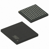
AT91SAM7XC512-CU Atmel, AT91SAM7XC512-CU Datasheet - Page 705

AT91SAM7XC512-CU
Manufacturer Part Number
AT91SAM7XC512-CU
Description
MCU ARM 512K HS FLASH 100-TFBGA
Manufacturer
Atmel
Series
AT91SAMr
Specifications of AT91SAM7XC512-CU
Core Processor
ARM7
Core Size
16/32-Bit
Speed
55MHz
Connectivity
CAN, Ethernet, I²C, SPI, SSC, UART/USART, USB
Peripherals
Brown-out Detect/Reset, DMA, POR, PWM, WDT
Number Of I /o
62
Program Memory Size
512KB (512K x 8)
Program Memory Type
FLASH
Ram Size
128K x 8
Voltage - Supply (vcc/vdd)
1.65 V ~ 1.95 V
Data Converters
A/D 8x10b
Oscillator Type
Internal
Operating Temperature
-40°C ~ 85°C
Package / Case
100-TFBGA
Processor Series
AT91SAMx
Core
ARM7TDMI
Data Bus Width
32 bit
Data Ram Size
128 KB
Interface Type
MII, SPI, TWI
Maximum Clock Frequency
55 MHz
Number Of Programmable I/os
62
Number Of Timers
3
Maximum Operating Temperature
+ 85 C
Mounting Style
SMD/SMT
3rd Party Development Tools
JTRACE-ARM-2M, KSK-AT91SAM7X-PL, MDK-ARM, RL-ARM, ULINK2
Development Tools By Supplier
AT91SAM-ICE, AT91-ISP, AT91SAM7XC-EK
Minimum Operating Temperature
- 40 C
On-chip Adc
10 bit, 8 Channel
For Use With
AT91SAM-ICE - EMULATOR FOR AT91 ARM7/ARM9AT91SAM7XC-EK - KIT EVAL FOR AT91SAM7XC256/128
Lead Free Status / RoHS Status
Lead free / RoHS Compliant
Eeprom Size
-
Lead Free Status / Rohs Status
Lead free / RoHS Compliant
Available stocks
Company
Part Number
Manufacturer
Quantity
Price
- Current page: 705 of 727
- Download datasheet (11Mb)
44.4.8.2
44.4.8.3
44.4.9
44.4.9.1
44.4.9.2
6209F–ATARM–17-Feb-09
Two-wire Interface (TWI)
SSC: Transmitter Limitations in Slave Mode
SSC: Transmitter Limitations in Slave Mode
TWI: Clock Divider
TWI: Disabling Does not Operate Correctly
If TK is programmed as output and TF is programmed as input, it is impossible to emit data
when the start of edge (rising or falling) of synchro has a Start Delay equal to zero.
None.
If TK is programmed as an input and TF is programmed as an output and requested to be set to
low/high during data emission, the Frame Synchro signal is generated one bit clock period after
the data start and one data bit is lost. This problem does not exist when generating a periodic
synchro.
The data need to be delayed for one bit clock period with an external assembly. In the following
schematic, TD, TK and NRST are AT91SAM7XC signals, TXD is the delayed data to connect to
the device.
The value of CLDIV x 2
must be less than or equal to 8191⋅
None.
Any transfer in progress is immediately frozen if the Control Register (TWI_CR) is written with
the bit MSDIS at 1. Furthermore, the status bits TXCOMP and TXRDY in the Status Register
(TWI_SR) are not reset.
Problem Fix/Workaround
Problem Fix/Workaround
Problem Fix/Workaround
Problem Fix/Workaround
AT91SAM7XC512/256/128 Preliminary
CKDIV
must be less than or equal to 8191, the value of CHDIV x 2
CKDIV
705
Related parts for AT91SAM7XC512-CU
Image
Part Number
Description
Manufacturer
Datasheet
Request
R

Part Number:
Description:
KIT EVAL FOR AT91SAM7XC256/128
Manufacturer:
Atmel
Datasheet:

Part Number:
Description:
KIT EVAL FOR AT91SAM7X256/128
Manufacturer:
Atmel
Datasheet:

Part Number:
Description:
MCU, MPU & DSP Development Tools KICKSTART KIT ATMEL AT91SAM7X
Manufacturer:
IAR Systems

Part Number:
Description:
MCU ARM9 64K SRAM 144-LFBGA
Manufacturer:
Atmel
Datasheet:

Part Number:
Description:
IC ARM7 MCU FLASH 256K 100LQFP
Manufacturer:
Atmel
Datasheet:

Part Number:
Description:
IC ARM9 MPU 217-LFBGA
Manufacturer:
Atmel
Datasheet:

Part Number:
Description:
MCU ARM9 ULTRA LOW PWR 217-LFBGA
Manufacturer:
Atmel
Datasheet:

Part Number:
Description:
MCU ARM9 324-TFBGA
Manufacturer:
Atmel
Datasheet:

Part Number:
Description:
IC MCU ARM9 SAMPLING 217CBGA
Manufacturer:
Atmel
Datasheet:

Part Number:
Description:
IC ARM9 MCU 217-LFBGA
Manufacturer:
Atmel
Datasheet:

Part Number:
Description:
IC ARM9 MCU 208-PQFP
Manufacturer:
Atmel
Datasheet:

Part Number:
Description:
MCU ARM 512K HS FLASH 100-LQFP
Manufacturer:
Atmel
Datasheet:

Part Number:
Description:
MCU ARM 512K HS FLASH 100-TFBGA
Manufacturer:
Atmel
Datasheet:

Part Number:
Description:
IC ARM9 MCU 200 MHZ 324-TFBGA
Manufacturer:
Atmel
Datasheet:

Part Number:
Description:
IC ARM MCU 16BIT 128K 256BGA
Manufacturer:
Atmel
Datasheet:


