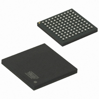
AT91SAM7XC512-CU Atmel, AT91SAM7XC512-CU Datasheet - Page 131

AT91SAM7XC512-CU
Manufacturer Part Number
AT91SAM7XC512-CU
Description
MCU ARM 512K HS FLASH 100-TFBGA
Manufacturer
Atmel
Series
AT91SAMr
Specifications of AT91SAM7XC512-CU
Core Processor
ARM7
Core Size
16/32-Bit
Speed
55MHz
Connectivity
CAN, Ethernet, I²C, SPI, SSC, UART/USART, USB
Peripherals
Brown-out Detect/Reset, DMA, POR, PWM, WDT
Number Of I /o
62
Program Memory Size
512KB (512K x 8)
Program Memory Type
FLASH
Ram Size
128K x 8
Voltage - Supply (vcc/vdd)
1.65 V ~ 1.95 V
Data Converters
A/D 8x10b
Oscillator Type
Internal
Operating Temperature
-40°C ~ 85°C
Package / Case
100-TFBGA
Processor Series
AT91SAMx
Core
ARM7TDMI
Data Bus Width
32 bit
Data Ram Size
128 KB
Interface Type
MII, SPI, TWI
Maximum Clock Frequency
55 MHz
Number Of Programmable I/os
62
Number Of Timers
3
Maximum Operating Temperature
+ 85 C
Mounting Style
SMD/SMT
3rd Party Development Tools
JTRACE-ARM-2M, KSK-AT91SAM7X-PL, MDK-ARM, RL-ARM, ULINK2
Development Tools By Supplier
AT91SAM-ICE, AT91-ISP, AT91SAM7XC-EK
Minimum Operating Temperature
- 40 C
On-chip Adc
10 bit, 8 Channel
For Use With
AT91SAM-ICE - EMULATOR FOR AT91 ARM7/ARM9AT91SAM7XC-EK - KIT EVAL FOR AT91SAM7XC256/128
Lead Free Status / RoHS Status
Lead free / RoHS Compliant
Eeprom Size
-
Lead Free Status / Rohs Status
Lead free / RoHS Compliant
Available stocks
Company
Part Number
Manufacturer
Quantity
Price
- Current page: 131 of 727
- Download datasheet (11Mb)
20. Embedded Flash Controller (EFC)
20.1
20.2
20.2.1
6209F–ATARM–17-Feb-09
Overview
Functional Description
Embedded Flash Organization
The Embedded Flash Controller (EFC ) is a part of the Memory Controller and ensures the inter-
face of the Flash block with the 32-bit internal bus. It increases performance in Thumb Mode for
Code Fetch with its system of 32-bit buffers. It also manages the programming, erasing, locking
and unlocking sequences using a full set of commands.
The AT91SAM7XC512 is equipped with two EFCs, EFC0 and EFC1. EFC1 does not feature the
Security bit and GPNVM bits. The Security and GPNVM bits embedded only on EFC0 apply to
the two blocks in the AT91SAM7XC512.
The Embedded Flash interfaces directly to the 32-bit internal bus. It is composed of several
interfaces:
The Embedded Flash size, the page size and the lock region organization are described in the
product definition section.
Table 20-1.
AT91SAM7XC512 AT91SAM7XC256 AT91SAM7XC128 Denomination
• One memory plane organized in several pages of the same size
• Two 32-bit read buffers used for code read optimization (see
• One write buffer that manages page programming. The write buffer size is equal to the page
• Several lock bits used to protect write and erase operations on lock regions. A lock region is
• Several general-purpose NVM bits. Each bit controls a specific feature in the device. Refer to
132).
size. This buffer is write-only and accessible all along the 1 MByte address space, so that
each word can be written to its final address (see
composed of several consecutive pages, and each lock region has its associated lock bit.
the product definition section to get the GPNVM assignment.
32
3
Product Specific Lock and General-purpose NVM Bits
AT91SAM7XC512/256/128 Preliminary
16
3
3
8
“Write Operations” on page
Number of General-purpose NVM bits
Number of Lock Bits
“Read Operations” on page
134).
131
Related parts for AT91SAM7XC512-CU
Image
Part Number
Description
Manufacturer
Datasheet
Request
R

Part Number:
Description:
KIT EVAL FOR AT91SAM7XC256/128
Manufacturer:
Atmel
Datasheet:

Part Number:
Description:
KIT EVAL FOR AT91SAM7X256/128
Manufacturer:
Atmel
Datasheet:

Part Number:
Description:
MCU, MPU & DSP Development Tools KICKSTART KIT ATMEL AT91SAM7X
Manufacturer:
IAR Systems

Part Number:
Description:
MCU ARM9 64K SRAM 144-LFBGA
Manufacturer:
Atmel
Datasheet:

Part Number:
Description:
IC ARM7 MCU FLASH 256K 100LQFP
Manufacturer:
Atmel
Datasheet:

Part Number:
Description:
IC ARM9 MPU 217-LFBGA
Manufacturer:
Atmel
Datasheet:

Part Number:
Description:
MCU ARM9 ULTRA LOW PWR 217-LFBGA
Manufacturer:
Atmel
Datasheet:

Part Number:
Description:
MCU ARM9 324-TFBGA
Manufacturer:
Atmel
Datasheet:

Part Number:
Description:
IC MCU ARM9 SAMPLING 217CBGA
Manufacturer:
Atmel
Datasheet:

Part Number:
Description:
IC ARM9 MCU 217-LFBGA
Manufacturer:
Atmel
Datasheet:

Part Number:
Description:
IC ARM9 MCU 208-PQFP
Manufacturer:
Atmel
Datasheet:

Part Number:
Description:
MCU ARM 512K HS FLASH 100-LQFP
Manufacturer:
Atmel
Datasheet:

Part Number:
Description:
MCU ARM 512K HS FLASH 100-TFBGA
Manufacturer:
Atmel
Datasheet:

Part Number:
Description:
IC ARM9 MCU 200 MHZ 324-TFBGA
Manufacturer:
Atmel
Datasheet:

Part Number:
Description:
IC ARM MCU 16BIT 128K 256BGA
Manufacturer:
Atmel
Datasheet:


