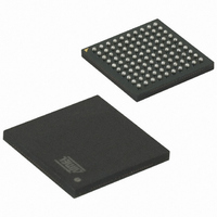
AT91SAM7XC512-CU Atmel, AT91SAM7XC512-CU Datasheet - Page 511

AT91SAM7XC512-CU
Manufacturer Part Number
AT91SAM7XC512-CU
Description
MCU ARM 512K HS FLASH 100-TFBGA
Manufacturer
Atmel
Series
AT91SAMr
Specifications of AT91SAM7XC512-CU
Core Processor
ARM7
Core Size
16/32-Bit
Speed
55MHz
Connectivity
CAN, Ethernet, I²C, SPI, SSC, UART/USART, USB
Peripherals
Brown-out Detect/Reset, DMA, POR, PWM, WDT
Number Of I /o
62
Program Memory Size
512KB (512K x 8)
Program Memory Type
FLASH
Ram Size
128K x 8
Voltage - Supply (vcc/vdd)
1.65 V ~ 1.95 V
Data Converters
A/D 8x10b
Oscillator Type
Internal
Operating Temperature
-40°C ~ 85°C
Package / Case
100-TFBGA
Processor Series
AT91SAMx
Core
ARM7TDMI
Data Bus Width
32 bit
Data Ram Size
128 KB
Interface Type
MII, SPI, TWI
Maximum Clock Frequency
55 MHz
Number Of Programmable I/os
62
Number Of Timers
3
Maximum Operating Temperature
+ 85 C
Mounting Style
SMD/SMT
3rd Party Development Tools
JTRACE-ARM-2M, KSK-AT91SAM7X-PL, MDK-ARM, RL-ARM, ULINK2
Development Tools By Supplier
AT91SAM-ICE, AT91-ISP, AT91SAM7XC-EK
Minimum Operating Temperature
- 40 C
On-chip Adc
10 bit, 8 Channel
For Use With
AT91SAM-ICE - EMULATOR FOR AT91 ARM7/ARM9AT91SAM7XC-EK - KIT EVAL FOR AT91SAM7XC256/128
Lead Free Status / RoHS Status
Lead free / RoHS Compliant
Eeprom Size
-
Lead Free Status / Rohs Status
Lead free / RoHS Compliant
Available stocks
Company
Part Number
Manufacturer
Quantity
Price
- Current page: 511 of 727
- Download datasheet (11Mb)
36.3.3.2
6209F–ATARM–17-Feb-09
If LOD = 1
If LOD = 0
If LOD = 1
PDC Mode
If the user does not want to read the output data registers between each encryption/decryption,
the DATRDY flag will not be cleared. If the DATRDY flag is not cleared, the user cannot know
the end of the following encryptions/decryptions.
The DATRDY flag is cleared when at least one Input Data Register is written, so before the start
of a new transfer (See
between consecutive encryptions/decryptions.
Figure 36-2. Manual and Auto Modes with LOD = 1
The end of the encryption/decryption is notified by the ENDRX (or RXBUFF) flag rise (see
36-3).
Figure 36-3. PDC Mode with LOD = 0
The user must first wait for the ENDTX (or TXBUFE) flag to rise, then for DATRDY to ensure that
the encryption/decryption is completed (see
In this case, no receive buffers are required.
The output data is only available on the Output Data Registers (AES_ODATAxR).
ENDRX (or RXBUFF)
DATRDY
Write AES_IDATAxR register(s) (Auto mode)
Write START bit in AES_CR (Manual mode)
Enable PDC Channels (Receive and Transmit Channels)
AT91SAM7XC512/256/128 Preliminary
Figure
or
Multiple Encryption or Decryption Processes
Encryption or Decryption Process
36-2). No more Output Data Register reads are necessary
Figure
36-4).
Write AES_IDATAxR register(s)
Figure
511
Related parts for AT91SAM7XC512-CU
Image
Part Number
Description
Manufacturer
Datasheet
Request
R

Part Number:
Description:
KIT EVAL FOR AT91SAM7XC256/128
Manufacturer:
Atmel
Datasheet:

Part Number:
Description:
KIT EVAL FOR AT91SAM7X256/128
Manufacturer:
Atmel
Datasheet:

Part Number:
Description:
MCU, MPU & DSP Development Tools KICKSTART KIT ATMEL AT91SAM7X
Manufacturer:
IAR Systems

Part Number:
Description:
MCU ARM9 64K SRAM 144-LFBGA
Manufacturer:
Atmel
Datasheet:

Part Number:
Description:
IC ARM7 MCU FLASH 256K 100LQFP
Manufacturer:
Atmel
Datasheet:

Part Number:
Description:
IC ARM9 MPU 217-LFBGA
Manufacturer:
Atmel
Datasheet:

Part Number:
Description:
MCU ARM9 ULTRA LOW PWR 217-LFBGA
Manufacturer:
Atmel
Datasheet:

Part Number:
Description:
MCU ARM9 324-TFBGA
Manufacturer:
Atmel
Datasheet:

Part Number:
Description:
IC MCU ARM9 SAMPLING 217CBGA
Manufacturer:
Atmel
Datasheet:

Part Number:
Description:
IC ARM9 MCU 217-LFBGA
Manufacturer:
Atmel
Datasheet:

Part Number:
Description:
IC ARM9 MCU 208-PQFP
Manufacturer:
Atmel
Datasheet:

Part Number:
Description:
MCU ARM 512K HS FLASH 100-LQFP
Manufacturer:
Atmel
Datasheet:

Part Number:
Description:
MCU ARM 512K HS FLASH 100-TFBGA
Manufacturer:
Atmel
Datasheet:

Part Number:
Description:
IC ARM9 MCU 200 MHZ 324-TFBGA
Manufacturer:
Atmel
Datasheet:

Part Number:
Description:
IC ARM MCU 16BIT 128K 256BGA
Manufacturer:
Atmel
Datasheet:


