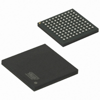
AT91SAM7XC512-CU Atmel, AT91SAM7XC512-CU Datasheet - Page 207

AT91SAM7XC512-CU
Manufacturer Part Number
AT91SAM7XC512-CU
Description
MCU ARM 512K HS FLASH 100-TFBGA
Manufacturer
Atmel
Series
AT91SAMr
Specifications of AT91SAM7XC512-CU
Core Processor
ARM7
Core Size
16/32-Bit
Speed
55MHz
Connectivity
CAN, Ethernet, I²C, SPI, SSC, UART/USART, USB
Peripherals
Brown-out Detect/Reset, DMA, POR, PWM, WDT
Number Of I /o
62
Program Memory Size
512KB (512K x 8)
Program Memory Type
FLASH
Ram Size
128K x 8
Voltage - Supply (vcc/vdd)
1.65 V ~ 1.95 V
Data Converters
A/D 8x10b
Oscillator Type
Internal
Operating Temperature
-40°C ~ 85°C
Package / Case
100-TFBGA
Processor Series
AT91SAMx
Core
ARM7TDMI
Data Bus Width
32 bit
Data Ram Size
128 KB
Interface Type
MII, SPI, TWI
Maximum Clock Frequency
55 MHz
Number Of Programmable I/os
62
Number Of Timers
3
Maximum Operating Temperature
+ 85 C
Mounting Style
SMD/SMT
3rd Party Development Tools
JTRACE-ARM-2M, KSK-AT91SAM7X-PL, MDK-ARM, RL-ARM, ULINK2
Development Tools By Supplier
AT91SAM-ICE, AT91-ISP, AT91SAM7XC-EK
Minimum Operating Temperature
- 40 C
On-chip Adc
10 bit, 8 Channel
For Use With
AT91SAM-ICE - EMULATOR FOR AT91 ARM7/ARM9AT91SAM7XC-EK - KIT EVAL FOR AT91SAM7XC256/128
Lead Free Status / RoHS Status
Lead free / RoHS Compliant
Eeprom Size
-
Lead Free Status / Rohs Status
Lead free / RoHS Compliant
Available stocks
Company
Part Number
Manufacturer
Quantity
Price
- Current page: 207 of 727
- Download datasheet (11Mb)
25.3.5
25.4
25.4.1
6209F–ATARM–17-Feb-09
Divider and PLL Block
Main Oscillator Bypass
PLL Filter
Slow Clock, so that the frequency of the crystal connected on the Main Oscillator can be
determined.
The user can input a clock on the device instead of connecting a crystal. In this case, the user
has to provide the external clock signal on the XIN pin. The input characteristics of the XIN pin
under these conditions are given in the product electrical characteristics section. The program-
mer has to be sure to set the OSCBYPASS bit to 1 and the MOSCEN bit to 0 in the Main OSC
register (CKGR_MOR) for the external clock to operate properly.
The PLL embeds an input divider to increase the accuracy of the resulting clock signals. How-
ever, the user must respect the PLL minimum input frequency when programming the divider.
Figure 25-3
Figure 25-3. Divider and PLL Block Diagram
The PLL requires connection to an external second-order filter through the PLLRC pin.
25-4
Figure 25-4. PLL Capacitors and Resistors
Values of R, C1 and C2 to be connected to the PLLRC pin must be calculated as a function of
the PLL input frequency, the PLL output frequency and the phase margin. A trade-off has to be
found between output signal overshoot and startup time.
shows a schematic of these filters.
shows the block diagram of the divider and PLL block.
MAINCK
AT91SAM7XC512/256/128 Preliminary
SLCK
C2
Divider
DIV
C1
R
PLLRC
GND
PLLCOUNT
Counter
PLLRC
PLL
MUL
PLL
PLL
OUT
LOCK
PLLCK
Figure
207
Related parts for AT91SAM7XC512-CU
Image
Part Number
Description
Manufacturer
Datasheet
Request
R

Part Number:
Description:
KIT EVAL FOR AT91SAM7XC256/128
Manufacturer:
Atmel
Datasheet:

Part Number:
Description:
KIT EVAL FOR AT91SAM7X256/128
Manufacturer:
Atmel
Datasheet:

Part Number:
Description:
MCU, MPU & DSP Development Tools KICKSTART KIT ATMEL AT91SAM7X
Manufacturer:
IAR Systems

Part Number:
Description:
MCU ARM9 64K SRAM 144-LFBGA
Manufacturer:
Atmel
Datasheet:

Part Number:
Description:
IC ARM7 MCU FLASH 256K 100LQFP
Manufacturer:
Atmel
Datasheet:

Part Number:
Description:
IC ARM9 MPU 217-LFBGA
Manufacturer:
Atmel
Datasheet:

Part Number:
Description:
MCU ARM9 ULTRA LOW PWR 217-LFBGA
Manufacturer:
Atmel
Datasheet:

Part Number:
Description:
MCU ARM9 324-TFBGA
Manufacturer:
Atmel
Datasheet:

Part Number:
Description:
IC MCU ARM9 SAMPLING 217CBGA
Manufacturer:
Atmel
Datasheet:

Part Number:
Description:
IC ARM9 MCU 217-LFBGA
Manufacturer:
Atmel
Datasheet:

Part Number:
Description:
IC ARM9 MCU 208-PQFP
Manufacturer:
Atmel
Datasheet:

Part Number:
Description:
MCU ARM 512K HS FLASH 100-LQFP
Manufacturer:
Atmel
Datasheet:

Part Number:
Description:
MCU ARM 512K HS FLASH 100-TFBGA
Manufacturer:
Atmel
Datasheet:

Part Number:
Description:
IC ARM9 MCU 200 MHZ 324-TFBGA
Manufacturer:
Atmel
Datasheet:

Part Number:
Description:
IC ARM MCU 16BIT 128K 256BGA
Manufacturer:
Atmel
Datasheet:


