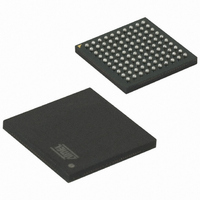
AT91SAM7XC512-CU Atmel, AT91SAM7XC512-CU Datasheet - Page 510

AT91SAM7XC512-CU
Manufacturer Part Number
AT91SAM7XC512-CU
Description
MCU ARM 512K HS FLASH 100-TFBGA
Manufacturer
Atmel
Series
AT91SAMr
Specifications of AT91SAM7XC512-CU
Core Processor
ARM7
Core Size
16/32-Bit
Speed
55MHz
Connectivity
CAN, Ethernet, I²C, SPI, SSC, UART/USART, USB
Peripherals
Brown-out Detect/Reset, DMA, POR, PWM, WDT
Number Of I /o
62
Program Memory Size
512KB (512K x 8)
Program Memory Type
FLASH
Ram Size
128K x 8
Voltage - Supply (vcc/vdd)
1.65 V ~ 1.95 V
Data Converters
A/D 8x10b
Oscillator Type
Internal
Operating Temperature
-40°C ~ 85°C
Package / Case
100-TFBGA
Processor Series
AT91SAMx
Core
ARM7TDMI
Data Bus Width
32 bit
Data Ram Size
128 KB
Interface Type
MII, SPI, TWI
Maximum Clock Frequency
55 MHz
Number Of Programmable I/os
62
Number Of Timers
3
Maximum Operating Temperature
+ 85 C
Mounting Style
SMD/SMT
3rd Party Development Tools
JTRACE-ARM-2M, KSK-AT91SAM7X-PL, MDK-ARM, RL-ARM, ULINK2
Development Tools By Supplier
AT91SAM-ICE, AT91-ISP, AT91SAM7XC-EK
Minimum Operating Temperature
- 40 C
On-chip Adc
10 bit, 8 Channel
For Use With
AT91SAM-ICE - EMULATOR FOR AT91 ARM7/ARM9AT91SAM7XC-EK - KIT EVAL FOR AT91SAM7XC256/128
Lead Free Status / RoHS Status
Lead free / RoHS Compliant
Eeprom Size
-
Lead Free Status / Rohs Status
Lead free / RoHS Compliant
Available stocks
Company
Part Number
Manufacturer
Quantity
Price
- Current page: 510 of 727
- Download datasheet (11Mb)
36.3.3
36.3.3.1
510
If LOD = 0
AT91SAM7XC512/256/128 Preliminary
Last Output Data Mode
Manual and Auto Modes
Note:
Note:
Note:
This mode is used to generate cryptographic checksums on data (MAC) by means of cipher
block chaining encryption algorithm (CBC-MAC algorithm for example).
After each end of encryption/decryption, the output data is available either on the output data
registers for Manual and Auto mode or at the address specified in the receive buffer pointer for
PDC mode (See
The Last Output Data bit (LOD) in the AES Mode Register (AES_MR) allows retrieval of only the
last data of several encryption/decryption processes.
Therefore, there is no need to define a read buffer in PDC mode.
This data is only available on the Output Data Registers (AES_ODATAxR).
The DATRDY flag is cleared when at least one of the Output Data Registers is read (See
36-1).
Figure 36-1. Manual and Auto Modes with LOD = 0
• Set the Transmit Pointer Register (AES_TPR) to the address where the data buffer to
• Set the Transmit and the Receive Counter Registers (AES_TCR and AES_RCR) to the same
• If not already done, set the bit ENDRX (or RXBUFF if the next pointers and counters are
• Enable the PDC in transmission and reception to start the processing (AES_PTCR).
• When the processing completes, the bit ENDRX (or RXBUFF) in the AES Interrupt Status
encrypt/decrypt is stored and the Receive Pointer Register (AES_RPR) where it must be
encrypted/decrypted.
value. This value must be a multiple of the data transfer type size (see
used) in the AES Interrupt Enable register (AES_IER), depending on whether an interrupt is
required or not at the end of processing.
Register (AES_ISR) raises. If an interrupt has been enabled by setting the corresponding bit
in AES_IER, the interrupt line of the AES is activated.
The Initialization Vector Registers concern all modes except ECB.
Transmit and receive buffers can be identical.
The same requirements are necessary for the Next Pointer(s) and Counter(s) of the PDC
(AES_TNPR, AES_RNPR, AES_TNCR, AES_RNCR).
DATRDY
Write AES_IDATAxR register(s) (Auto mode)
Write START bit in AES_CR (Manual mode)
Table 36-3 on page
or
Encryption or Decryption Process
512).
Read the AES_ODATAxR
Table
6209F–ATARM–17-Feb-09
36-2).
Figure
Related parts for AT91SAM7XC512-CU
Image
Part Number
Description
Manufacturer
Datasheet
Request
R

Part Number:
Description:
KIT EVAL FOR AT91SAM7XC256/128
Manufacturer:
Atmel
Datasheet:

Part Number:
Description:
KIT EVAL FOR AT91SAM7X256/128
Manufacturer:
Atmel
Datasheet:

Part Number:
Description:
MCU, MPU & DSP Development Tools KICKSTART KIT ATMEL AT91SAM7X
Manufacturer:
IAR Systems

Part Number:
Description:
MCU ARM9 64K SRAM 144-LFBGA
Manufacturer:
Atmel
Datasheet:

Part Number:
Description:
IC ARM7 MCU FLASH 256K 100LQFP
Manufacturer:
Atmel
Datasheet:

Part Number:
Description:
IC ARM9 MPU 217-LFBGA
Manufacturer:
Atmel
Datasheet:

Part Number:
Description:
MCU ARM9 ULTRA LOW PWR 217-LFBGA
Manufacturer:
Atmel
Datasheet:

Part Number:
Description:
MCU ARM9 324-TFBGA
Manufacturer:
Atmel
Datasheet:

Part Number:
Description:
IC MCU ARM9 SAMPLING 217CBGA
Manufacturer:
Atmel
Datasheet:

Part Number:
Description:
IC ARM9 MCU 217-LFBGA
Manufacturer:
Atmel
Datasheet:

Part Number:
Description:
IC ARM9 MCU 208-PQFP
Manufacturer:
Atmel
Datasheet:

Part Number:
Description:
MCU ARM 512K HS FLASH 100-LQFP
Manufacturer:
Atmel
Datasheet:

Part Number:
Description:
MCU ARM 512K HS FLASH 100-TFBGA
Manufacturer:
Atmel
Datasheet:

Part Number:
Description:
IC ARM9 MCU 200 MHZ 324-TFBGA
Manufacturer:
Atmel
Datasheet:

Part Number:
Description:
IC ARM MCU 16BIT 128K 256BGA
Manufacturer:
Atmel
Datasheet:


