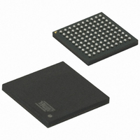
AT91SAM7XC512-CU Atmel, AT91SAM7XC512-CU Datasheet - Page 39

AT91SAM7XC512-CU
Manufacturer Part Number
AT91SAM7XC512-CU
Description
MCU ARM 512K HS FLASH 100-TFBGA
Manufacturer
Atmel
Series
AT91SAMr
Specifications of AT91SAM7XC512-CU
Core Processor
ARM7
Core Size
16/32-Bit
Speed
55MHz
Connectivity
CAN, Ethernet, I²C, SPI, SSC, UART/USART, USB
Peripherals
Brown-out Detect/Reset, DMA, POR, PWM, WDT
Number Of I /o
62
Program Memory Size
512KB (512K x 8)
Program Memory Type
FLASH
Ram Size
128K x 8
Voltage - Supply (vcc/vdd)
1.65 V ~ 1.95 V
Data Converters
A/D 8x10b
Oscillator Type
Internal
Operating Temperature
-40°C ~ 85°C
Package / Case
100-TFBGA
Processor Series
AT91SAMx
Core
ARM7TDMI
Data Bus Width
32 bit
Data Ram Size
128 KB
Interface Type
MII, SPI, TWI
Maximum Clock Frequency
55 MHz
Number Of Programmable I/os
62
Number Of Timers
3
Maximum Operating Temperature
+ 85 C
Mounting Style
SMD/SMT
3rd Party Development Tools
JTRACE-ARM-2M, KSK-AT91SAM7X-PL, MDK-ARM, RL-ARM, ULINK2
Development Tools By Supplier
AT91SAM-ICE, AT91-ISP, AT91SAM7XC-EK
Minimum Operating Temperature
- 40 C
On-chip Adc
10 bit, 8 Channel
For Use With
AT91SAM-ICE - EMULATOR FOR AT91 ARM7/ARM9AT91SAM7XC-EK - KIT EVAL FOR AT91SAM7XC256/128
Lead Free Status / RoHS Status
Lead free / RoHS Compliant
Eeprom Size
-
Lead Free Status / Rohs Status
Lead free / RoHS Compliant
Available stocks
Company
Part Number
Manufacturer
Quantity
Price
- Current page: 39 of 727
- Download datasheet (11Mb)
10.13 USB Device Port
10.14 CAN Controller
10.15 128-bit Advanced Encryption Standard
6209F–ATARM–17-Feb-09
•
•
•
• USB V2.0 full-speed compliant,12 Mbits per second
• Embedded USB V2.0 full-speed transceiver
• Embedded 1352-byte dual-port RAM for endpoints
• Six endpoints
• Suspend/resume logic
• Compliant with FIPS Publication 197, Advanced Encryption Standard (AES)
• 128-bit (AT91SAM7XC256/128) or 128-bit/192-bit/256-bit (AT91SAM7XC512) Cryptographic
• 12-clock Cycles Encryption/Decryption Processing Time (AT91SAM7XC256/128)
• 12/13/14-clock Cycles Encryption/Decryption Processing Time (AT91SAM7XC512)
• Support of the Five Standard Modes of Operation specified in the NIST Special Publication
Key
800-38A:
Fully compliant with CAN 2.0A and 2.0B
Bit rates up to 1Mbit/s
Eight object oriented mailboxes each with the following properties:
– Endpoint 0: 8 bytes
– Endpoint 1 and 2: 64 bytes ping-pong
– Endpoint 3: 64 bytes
– Endpoint 4 and 5: 256 bytes ping-pong
– Ping-pong Mode (two memory banks) for bulk endpoints
– CAN Specification 2.0 Part A or 2.0 Part B Programmable for each Message
– Object configurable to receive (with overwrite or not) or transmit
– Local tag and mask filters up to 29-bit identifier/channel
– 32-bit access to data registers for each mailbox data object
– Uses a 16-bit time stamp on receive and transmit message
– Hardware concatenation of ID unmasked bitfields to speedup family ID processing
– 16-bit internal timer for time stamping and network synchronization
– Programmable reception buffer length up to 8 mailbox objects
– Priority management between transmission mailboxes
– Autobaud and listening mode
– Low power mode and programmable wake-up on bus activity or by the application
– Data, remote, error and overload frame handling
– Electronic Codebook (ECB)
– Cipher Block Chaining (CBC)
– Cipher Feedback (CFB)
– Output Feedback (OFB)
AT91SAM7XC512/256/128 Preliminary
39
Related parts for AT91SAM7XC512-CU
Image
Part Number
Description
Manufacturer
Datasheet
Request
R

Part Number:
Description:
KIT EVAL FOR AT91SAM7XC256/128
Manufacturer:
Atmel
Datasheet:

Part Number:
Description:
KIT EVAL FOR AT91SAM7X256/128
Manufacturer:
Atmel
Datasheet:

Part Number:
Description:
MCU, MPU & DSP Development Tools KICKSTART KIT ATMEL AT91SAM7X
Manufacturer:
IAR Systems

Part Number:
Description:
MCU ARM9 64K SRAM 144-LFBGA
Manufacturer:
Atmel
Datasheet:

Part Number:
Description:
IC ARM7 MCU FLASH 256K 100LQFP
Manufacturer:
Atmel
Datasheet:

Part Number:
Description:
IC ARM9 MPU 217-LFBGA
Manufacturer:
Atmel
Datasheet:

Part Number:
Description:
MCU ARM9 ULTRA LOW PWR 217-LFBGA
Manufacturer:
Atmel
Datasheet:

Part Number:
Description:
MCU ARM9 324-TFBGA
Manufacturer:
Atmel
Datasheet:

Part Number:
Description:
IC MCU ARM9 SAMPLING 217CBGA
Manufacturer:
Atmel
Datasheet:

Part Number:
Description:
IC ARM9 MCU 217-LFBGA
Manufacturer:
Atmel
Datasheet:

Part Number:
Description:
IC ARM9 MCU 208-PQFP
Manufacturer:
Atmel
Datasheet:

Part Number:
Description:
MCU ARM 512K HS FLASH 100-LQFP
Manufacturer:
Atmel
Datasheet:

Part Number:
Description:
MCU ARM 512K HS FLASH 100-TFBGA
Manufacturer:
Atmel
Datasheet:

Part Number:
Description:
IC ARM9 MCU 200 MHZ 324-TFBGA
Manufacturer:
Atmel
Datasheet:

Part Number:
Description:
IC ARM MCU 16BIT 128K 256BGA
Manufacturer:
Atmel
Datasheet:


