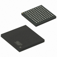
AT91SAM7XC512-CU Atmel, AT91SAM7XC512-CU Datasheet - Page 509

AT91SAM7XC512-CU
Manufacturer Part Number
AT91SAM7XC512-CU
Description
MCU ARM 512K HS FLASH 100-TFBGA
Manufacturer
Atmel
Series
AT91SAMr
Specifications of AT91SAM7XC512-CU
Core Processor
ARM7
Core Size
16/32-Bit
Speed
55MHz
Connectivity
CAN, Ethernet, I²C, SPI, SSC, UART/USART, USB
Peripherals
Brown-out Detect/Reset, DMA, POR, PWM, WDT
Number Of I /o
62
Program Memory Size
512KB (512K x 8)
Program Memory Type
FLASH
Ram Size
128K x 8
Voltage - Supply (vcc/vdd)
1.65 V ~ 1.95 V
Data Converters
A/D 8x10b
Oscillator Type
Internal
Operating Temperature
-40°C ~ 85°C
Package / Case
100-TFBGA
Processor Series
AT91SAMx
Core
ARM7TDMI
Data Bus Width
32 bit
Data Ram Size
128 KB
Interface Type
MII, SPI, TWI
Maximum Clock Frequency
55 MHz
Number Of Programmable I/os
62
Number Of Timers
3
Maximum Operating Temperature
+ 85 C
Mounting Style
SMD/SMT
3rd Party Development Tools
JTRACE-ARM-2M, KSK-AT91SAM7X-PL, MDK-ARM, RL-ARM, ULINK2
Development Tools By Supplier
AT91SAM-ICE, AT91-ISP, AT91SAM7XC-EK
Minimum Operating Temperature
- 40 C
On-chip Adc
10 bit, 8 Channel
For Use With
AT91SAM-ICE - EMULATOR FOR AT91 ARM7/ARM9AT91SAM7XC-EK - KIT EVAL FOR AT91SAM7XC256/128
Lead Free Status / RoHS Status
Lead free / RoHS Compliant
Eeprom Size
-
Lead Free Status / Rohs Status
Lead free / RoHS Compliant
Available stocks
Company
Part Number
Manufacturer
Quantity
Price
- Current page: 509 of 727
- Download datasheet (11Mb)
36.3.2.2
36.3.2.3
6209F–ATARM–17-Feb-09
Auto Mode
PDC Mode
Table 36-1.
Note:
Note:
The Auto Mode is similar to the manual one, except that in this mode, as soon as the correct
number of Input Data registers is written, processing is automatically started without any action
in the Control Register.
The Peripheral DMA Controller (PDC) can be used in association with the AES to perform an
encryption/decryption of a buffer without any action by the software during processing.
In this starting mode, the type of the data transfer (byte, half-word or word) depends on the oper-
ation mode.
Table 36-2.
The sequence is as follows:
• Set the START bit in the AES Control register AES_CR to begin the encryption or the
• When processing completes, the bit DATRDY in the AES Interrupt Status Register
• When the software reads one of the Output Data Registers (AES_ODATAxR), the DATRDY
• Write the 128-bit/192-bit/256-bit key in the Key Registers (AES_KEYWxR).
• Write the initialization vector (or counter) in the Initialization Vector Registers (AES_IVxR).
decryption process.
(AES_ISR) raises. If an interrupt has been enabled by setting the bit DATRDY in AES_IER,
the interrupt line of the AES is activated.
bit is automatically cleared.
Operation Mode
In 64-bit CFB mode, writing to AES_IDATA3R and AES_IDATA4R registers is not allowed and may
lead to errors in processing.
In 32-, 16- and 8-bit CFB modes, writing to AES_IDATA2R, AES_IDATA3R and AES_IDATA4R
registers is not allowed and may lead to errors in processing.
16-bit CFB
8-bit CFB
CTR
Operation Mode
CFB 128-bit
CFB 64-bit
CFB 32-bit
CFB 16-bit
Authorized Input Data Registers (Continued)
Data Transfer Type for the Different Operation Modes
CFB 8-bit
CBC
ECB
OFB
CTR
AT91SAM7XC512/256/128 Preliminary
Input Data Registers to Write
AES_IDATA1R
AES_IDATA1R
Data Transfer Type (PDC)
All
Half-word
Word
Word
Word
Word
Word
Word
Word
Byte
509
Related parts for AT91SAM7XC512-CU
Image
Part Number
Description
Manufacturer
Datasheet
Request
R

Part Number:
Description:
KIT EVAL FOR AT91SAM7XC256/128
Manufacturer:
Atmel
Datasheet:

Part Number:
Description:
KIT EVAL FOR AT91SAM7X256/128
Manufacturer:
Atmel
Datasheet:

Part Number:
Description:
MCU, MPU & DSP Development Tools KICKSTART KIT ATMEL AT91SAM7X
Manufacturer:
IAR Systems

Part Number:
Description:
MCU ARM9 64K SRAM 144-LFBGA
Manufacturer:
Atmel
Datasheet:

Part Number:
Description:
IC ARM7 MCU FLASH 256K 100LQFP
Manufacturer:
Atmel
Datasheet:

Part Number:
Description:
IC ARM9 MPU 217-LFBGA
Manufacturer:
Atmel
Datasheet:

Part Number:
Description:
MCU ARM9 ULTRA LOW PWR 217-LFBGA
Manufacturer:
Atmel
Datasheet:

Part Number:
Description:
MCU ARM9 324-TFBGA
Manufacturer:
Atmel
Datasheet:

Part Number:
Description:
IC MCU ARM9 SAMPLING 217CBGA
Manufacturer:
Atmel
Datasheet:

Part Number:
Description:
IC ARM9 MCU 217-LFBGA
Manufacturer:
Atmel
Datasheet:

Part Number:
Description:
IC ARM9 MCU 208-PQFP
Manufacturer:
Atmel
Datasheet:

Part Number:
Description:
MCU ARM 512K HS FLASH 100-LQFP
Manufacturer:
Atmel
Datasheet:

Part Number:
Description:
MCU ARM 512K HS FLASH 100-TFBGA
Manufacturer:
Atmel
Datasheet:

Part Number:
Description:
IC ARM9 MCU 200 MHZ 324-TFBGA
Manufacturer:
Atmel
Datasheet:

Part Number:
Description:
IC ARM MCU 16BIT 128K 256BGA
Manufacturer:
Atmel
Datasheet:


