NNDK-MOD5272-KIT NetBurner Inc, NNDK-MOD5272-KIT Datasheet - Page 519
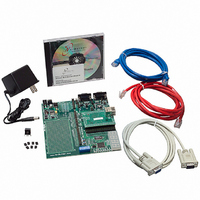
NNDK-MOD5272-KIT
Manufacturer Part Number
NNDK-MOD5272-KIT
Description
KIT DEVELOP NETWORK FOR MOD5272
Manufacturer
NetBurner Inc
Series
ColdFire®r
Datasheets
1.MOD5272-100IR.pdf
(2 pages)
2.MOD5272-100IR.pdf
(550 pages)
3.NNDK-MOD5282-KIT.pdf
(2 pages)
Specifications of NNDK-MOD5272-KIT
Main Purpose
*
Embedded
*
Utilized Ic / Part
MOD5272
Primary Attributes
*
Secondary Attributes
*
Processor To Be Evaluated
MOD5272
Interface Type
RS-232, RS-485, USB
Lead Free Status / RoHS Status
Contains lead / RoHS non-compliant
Lead Free Status / RoHS Status
Lead free / RoHS Compliant, Contains lead / RoHS non-compliant
Other names
528-1001


MOTOROLA
23.10 General-Purpose I/O Port AC Timing
Table 23-21 lists GPIO port timings.
Figure 23-21 shows GPIO timings listed in Table 23-21.
23.11 USB Interface AC Timing Specifications
Table 23-22 lists USB interface timings.
Name
US2
US3
US1
US4
US5
2
2
Specifications
USB_CLK frequency of operation
USB_CLK fall time (from V
USB_CLK rise time (from V
USB_CLK duty cycle (measured at 1.5 V)
USB Inputs (USB_RP, USB_RN, USB_RxD) setup time to USB_CLK (rising)
1
Table 23-21. General-Purpose I/O Port AC Timing Specifications
Name
All timing references to SDCLK are given to its rising edge when bit 3 of the SDRAM
control register is 0.
G1
G2
G3
G4
Table 23-22. USB Interface AC Timing Specifications
PORTx input setup time to SDCLK (rising)
PORTx input hold time from SDCLK (rising)
SDCLK to PORTx output valid
SDCLK to PORTx output invalid (output hold)
Figure 23-21. General-Purpose I/O Port Timing
PORTx OUT
Chapter 23. Electrical Characteristics
h
l
PORTx IN
= 2.4V to V
= 0.5V to V
Characteristic
SDCLK
1
Characteristic
l
h
= 0.5V)
= 2.4V)
P1
1
P3
General-Purpose I/O Port AC Timing Specifications
Min
—
6
0
1
P2
0–66 MHz
P4
Max
11.5
—
—
—
Min
48-66 MHz
48
45
—
—
6
Unit
nS
nS
nS
nS
Max
48
55
—
2
2
MHz
23-25
Unit
nS
nS
nS
%
Related parts for NNDK-MOD5272-KIT
Image
Part Number
Description
Manufacturer
Datasheet
Request
R

Part Number:
Description:
BOARD SERIAL-ETHERNET 512K FLASH
Manufacturer:
NetBurner Inc
Datasheet:

Part Number:
Description:
PROCESSOR MODULE FLASH MOD5272
Manufacturer:
NetBurner Inc
Datasheet:

Part Number:
Description:
PROCESSOR MODULE 512KB FLASH
Manufacturer:
NetBurner Inc
Datasheet:

Part Number:
Description:
DUAL PORT SERIAL-ETHERNET
Manufacturer:
NetBurner Inc
Datasheet:

Part Number:
Description:
PROCESSOR MODULE FLASH
Manufacturer:
NetBurner Inc
Datasheet:

Part Number:
Description:
PROCESSOR MODULE 512KB FLASH
Manufacturer:
NetBurner Inc
Datasheet:

Part Number:
Description:
MOD5234 10/100 ETHERNET MODULE
Manufacturer:
NetBurner Inc
Datasheet:

Part Number:
Description:
KIT DEVELOP NETWORK FOR MOD5282
Manufacturer:
NetBurner Inc
Datasheet:

Part Number:
Description:
DUAL PORT SERIAL-ETHERNET
Manufacturer:
NetBurner Inc
Datasheet:

Part Number:
Description:
Ethernet Modules & Development Tools 32 Bit 66MHz 40 Pin DIP Industrial Temp
Manufacturer:
NetBurner Inc
Datasheet:

Part Number:
Description:
Ethernet Modules & Development Tools MOD5213 DEVELOPMENT KIT
Manufacturer:
NetBurner Inc

Part Number:
Description:
Ethernet Modules & Development Tools DUAL PORT SERIAL EHTERNET DEVICE
Manufacturer:
NetBurner Inc
Datasheet:

Part Number:
Description:
Ethernet ICs 32bit 147MHz CAN-to- Ethnt Device IndTemp
Manufacturer:
NetBurner Inc
Datasheet: