NNDK-MOD5272-KIT NetBurner Inc, NNDK-MOD5272-KIT Datasheet - Page 450
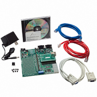
NNDK-MOD5272-KIT
Manufacturer Part Number
NNDK-MOD5272-KIT
Description
KIT DEVELOP NETWORK FOR MOD5272
Manufacturer
NetBurner Inc
Series
ColdFire®r
Datasheets
1.MOD5272-100IR.pdf
(2 pages)
2.MOD5272-100IR.pdf
(550 pages)
3.NNDK-MOD5282-KIT.pdf
(2 pages)
Specifications of NNDK-MOD5272-KIT
Main Purpose
*
Embedded
*
Utilized Ic / Part
MOD5272
Primary Attributes
*
Secondary Attributes
*
Processor To Be Evaluated
MOD5272
Interface Type
RS-232, RS-485, USB
Lead Free Status / RoHS Status
Contains lead / RoHS non-compliant
Lead Free Status / RoHS Status
Lead free / RoHS Compliant, Contains lead / RoHS non-compliant
Other names
528-1001


JTAG Test Access Port and BDM Debug Port
19.16.3.4 INT4 and Port 3 GCI/IDL Data In (INT4/DIN3)
IDL mode: This pin can be configured as a dedicated input, DIN3, for clocking data into
IDL port 3. Data is clocked into DIN3 on the falling edge of DCL1. Data is clocked into
DIN3 on the falling edge of DCL1. This is done by setting a bit in the PLIC module
configuration register. Note that the appropriate bits must be set in the pin configuration
register to reassign this pin from the interrupt module to the PLIC module.
GCI mode: This pin can be configured as a dedicated input, DIN3, for clocking data into
GCI port 3. DCL1 is twice the bit rate, that is, two clocks per data bit. This is done by setting
a bit in the PLIC module configuration register. Note that the appropriate bits must be set
in the pin configuration register to reassign this spin from the interrupt module to the PLIC
module.
Interrupt mode: This signal can be configured as interrupt input 4.
19.17 JTAG Test Access Port and BDM Debug Port
The MCF5272 supports the Motorola background debug mode (BDM) for ColdFire
processors. It also supports a JTAG test interface.
The following signals do not support JTAG due to the critical timing required to support
SDRAM memory: BS[3:0], RAS0, CAS0, SDCLK, SDCLKE, SDRAMCS/CS7, SDWE,
A10_PRECHG, SDBA[1:0], D[31:0], A[15:0].
19.17.1 Test Clock (TCK/PSTCLK)
JTAG mode: TCK is the dedicated JTAG test logic clock, independent of the CPU system
clock. This input provides a clock for on-board test logic defined by the IEEE 1149.1
standard.
TCK should be grounded if the JTAG port is not used and MTMOD is tied low.
BDM mode: PSTCLK is an output at the same frequency as the CPU clock. It is used for
indicating valid processor status data on the PST and DDATA pins.
19.17.2 Test Mode Select and Force Breakpoint (TMS/BKPT)
JTAG mode: The TMS input controls test mode operations for on-board test logic defined
by the IEEE 1149.1 standard. Connecting TMS to VDD disables the test controller, making
all JTAG circuits transparent to the system.
BDM mode: The hardware breakpoint input, BKPT, requires a 10-KΩ pullup resistor.
19-36
MCF5272 User’s Manual
MOTOROLA
Related parts for NNDK-MOD5272-KIT
Image
Part Number
Description
Manufacturer
Datasheet
Request
R

Part Number:
Description:
BOARD SERIAL-ETHERNET 512K FLASH
Manufacturer:
NetBurner Inc
Datasheet:

Part Number:
Description:
PROCESSOR MODULE FLASH MOD5272
Manufacturer:
NetBurner Inc
Datasheet:

Part Number:
Description:
PROCESSOR MODULE 512KB FLASH
Manufacturer:
NetBurner Inc
Datasheet:

Part Number:
Description:
DUAL PORT SERIAL-ETHERNET
Manufacturer:
NetBurner Inc
Datasheet:

Part Number:
Description:
PROCESSOR MODULE FLASH
Manufacturer:
NetBurner Inc
Datasheet:

Part Number:
Description:
PROCESSOR MODULE 512KB FLASH
Manufacturer:
NetBurner Inc
Datasheet:

Part Number:
Description:
MOD5234 10/100 ETHERNET MODULE
Manufacturer:
NetBurner Inc
Datasheet:

Part Number:
Description:
KIT DEVELOP NETWORK FOR MOD5282
Manufacturer:
NetBurner Inc
Datasheet:

Part Number:
Description:
DUAL PORT SERIAL-ETHERNET
Manufacturer:
NetBurner Inc
Datasheet:

Part Number:
Description:
Ethernet Modules & Development Tools 32 Bit 66MHz 40 Pin DIP Industrial Temp
Manufacturer:
NetBurner Inc
Datasheet:

Part Number:
Description:
Ethernet Modules & Development Tools MOD5213 DEVELOPMENT KIT
Manufacturer:
NetBurner Inc

Part Number:
Description:
Ethernet Modules & Development Tools DUAL PORT SERIAL EHTERNET DEVICE
Manufacturer:
NetBurner Inc
Datasheet:

Part Number:
Description:
Ethernet ICs 32bit 147MHz CAN-to- Ethnt Device IndTemp
Manufacturer:
NetBurner Inc
Datasheet: