NNDK-MOD5272-KIT NetBurner Inc, NNDK-MOD5272-KIT Datasheet - Page 397
NNDK-MOD5272-KIT
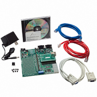
Manufacturer Part Number
NNDK-MOD5272-KIT
Description
KIT DEVELOP NETWORK FOR MOD5272
Manufacturer
NetBurner Inc
Series
ColdFire®r
Datasheets
1.MOD5272-100IR.pdf
(2 pages)
2.MOD5272-100IR.pdf
(550 pages)
3.NNDK-MOD5282-KIT.pdf
(2 pages)
Specifications of NNDK-MOD5272-KIT
Main Purpose
*
Embedded
*
Utilized Ic / Part
MOD5272
Primary Attributes
*
Secondary Attributes
*
Processor To Be Evaluated
MOD5272
Interface Type
RS-232, RS-485, USB
Lead Free Status / RoHS Status
Contains lead / RoHS non-compliant
Lead Free Status / RoHS Status
Lead free / RoHS Compliant, Contains lead / RoHS non-compliant
Other names
528-1001


MOTOROLA
Chapter 17
General Purpose I/O Module
This chapter describes the operation and programming model of the three
general-purpose I/O (GPIO) ports on the MCF5272. It includes details about pin
assignment, direction-control, and data registers..
17.1 Overview
The MCF5272 provides up to 48 general-purpose I/O signals. The GPIO signal
multiplexing is shown in Table 17-1. All GPIO pins are individually programmable as
inputs or outputs. At reset, all configurable multifunction GPIO pins default to general
purpose inputs and all multifunction pins that are not shared with a GPIO pin default to high
impedance. To avoid indeterminate read values and reduce power consumption, internal
pull-up resistors are active immediately upon reset, and remain active until the
corresponding port direction registers are programmed.
The general-purpose I/O signals are configured as three ports, each having up to 16 signals.
These three general-purpose I/O ports are shared with other signals as follows:
Control registers for each port select the function (GPIO or peripheral pin) assigned to each
pin. Pins can have as many as four functions including GPIO. There is no configuration
register for GPIO port C because its pins are configured by WSEL during device reset.
An additional port, port D, has only a control register which is used to configure the pins
that are not multiplexed with any GPIO signals.
PA[6:0]
PA7
PA[15:8]
PB[7:0]
PB[15:8]
PC[15:0]
GPIO Signal
external USB transceiver interface signals
QSPI_CS3 and DOUT3
PLIC TDM ports 0 and 1
UART1 signals and the bus control signal TA
Ethernet controller signals
data bus signals D[15:0]. These are only available (as GPIO) when the device is
configured for 16-bit data bus mode using the WSEL signal
Table 17-1. GPIO Signal Multiplexing
Chapter 17. General Purpose I/O Module
Also Multiplexed on the Same Pins
17-1
Related parts for NNDK-MOD5272-KIT
Image
Part Number
Description
Manufacturer
Datasheet
Request
R

Part Number:
Description:
BOARD SERIAL-ETHERNET 512K FLASH
Manufacturer:
NetBurner Inc
Datasheet:

Part Number:
Description:
PROCESSOR MODULE FLASH MOD5272
Manufacturer:
NetBurner Inc
Datasheet:

Part Number:
Description:
PROCESSOR MODULE 512KB FLASH
Manufacturer:
NetBurner Inc
Datasheet:

Part Number:
Description:
DUAL PORT SERIAL-ETHERNET
Manufacturer:
NetBurner Inc
Datasheet:

Part Number:
Description:
PROCESSOR MODULE FLASH
Manufacturer:
NetBurner Inc
Datasheet:

Part Number:
Description:
PROCESSOR MODULE 512KB FLASH
Manufacturer:
NetBurner Inc
Datasheet:

Part Number:
Description:
MOD5234 10/100 ETHERNET MODULE
Manufacturer:
NetBurner Inc
Datasheet:

Part Number:
Description:
KIT DEVELOP NETWORK FOR MOD5282
Manufacturer:
NetBurner Inc
Datasheet:

Part Number:
Description:
DUAL PORT SERIAL-ETHERNET
Manufacturer:
NetBurner Inc
Datasheet:

Part Number:
Description:
Ethernet Modules & Development Tools 32 Bit 66MHz 40 Pin DIP Industrial Temp
Manufacturer:
NetBurner Inc
Datasheet:

Part Number:
Description:
Ethernet Modules & Development Tools MOD5213 DEVELOPMENT KIT
Manufacturer:
NetBurner Inc

Part Number:
Description:
Ethernet Modules & Development Tools DUAL PORT SERIAL EHTERNET DEVICE
Manufacturer:
NetBurner Inc
Datasheet:

Part Number:
Description:
Ethernet ICs 32bit 147MHz CAN-to- Ethnt Device IndTemp
Manufacturer:
NetBurner Inc
Datasheet: