NNDK-MOD5272-KIT NetBurner Inc, NNDK-MOD5272-KIT Datasheet - Page 342
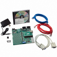
NNDK-MOD5272-KIT
Manufacturer Part Number
NNDK-MOD5272-KIT
Description
KIT DEVELOP NETWORK FOR MOD5272
Manufacturer
NetBurner Inc
Series
ColdFire®r
Datasheets
1.MOD5272-100IR.pdf
(2 pages)
2.MOD5272-100IR.pdf
(550 pages)
3.NNDK-MOD5282-KIT.pdf
(2 pages)
Specifications of NNDK-MOD5272-KIT
Main Purpose
*
Embedded
*
Utilized Ic / Part
MOD5272
Primary Attributes
*
Secondary Attributes
*
Processor To Be Evaluated
MOD5272
Interface Type
RS-232, RS-485, USB
Lead Free Status / RoHS Status
Contains lead / RoHS non-compliant
Lead Free Status / RoHS Status
Lead free / RoHS Compliant, Contains lead / RoHS non-compliant
Other names
528-1001


Operation
Execution continues at the internal pointer address unless the QWR[NEWQP] value is
changed. After each command is executed, QWR[ENDQP] and QWR[CPTQP] are
compared. When a match occurs, QIR[SPIF] is set and the QSPI stops unless wraparound
mode is enabled. Setting QWR[WREN] enables wraparound mode.
QWR[NEWQP] is cleared at reset. When the QSPI is enabled, execution begins at address
0x0 unless another value has been written into QWR[NEWQP]. QWR[ENDQP] is cleared
at reset but is changed to show the last queue entry before the QSPI is enabled.
QWR[NEWQP] and QWR[ENDQP] can be written at any time. When the QWR[NEWQP]
value changes, the internal pointer value also changes unless a transfer is in progress, in
which case the transfer completes normally. Leaving QWR[NEWQP] and QWR[ENDQP]
set to 0x0 causes a single transfer to occur when the QSPI is enabled.
Data is transferred relative to QSPI_CLK which can be generated in any one of four
combinations of phase and polarity using QMR[CPHA, CPOL]. Data is transferred most
significant bit (msb) first. The number of bits transferred defaults to eight, but can be set to
any value from 8 to 16 by writing a value into the BITSE field of the command RAM,
QCR[BITSE] .
14.4.1 QSPI RAM
The QSPI contains an 80-byte block of static RAM that can be accessed by both the user
and the QSPI. This RAM does not appear in the MCF5272 memory map because it can only
be accessed by the user indirectly through the QSPI address register (QAR) and the QSPI
data register (QDR). The RAM is divided into three segments with 16 addresses each:
The transmit and command RAM are write-only by the user. The receive RAM is read-only
by the user. Figure 14-2 shows the RAM configuration. The RAM contents are undefined
immediately after a reset.
The command and data RAM in the QSPI is indirectly accessible with QDR and QAR as
48 separate locations that comprise 16 words of transmit data, 16 words of receive data and
16 bytes of commands.
A write to QDR causes data to be written to the RAM entry specified by QAR[ADDR] and
causes the value in QAR to increment. Correspondingly, a read at QDR returns the data in
the RAM at the address specified by QAR[ADDR]. This also causes QAR to increment. A
read access requires a single wait state.
14-4
• receive data RAM, the initial destination for all incoming data
• transmit data RAM, a buffer for all out-bound data
• command RAM, where commands are loaded
MCF5272 User’s Manual
MOTOROLA
Related parts for NNDK-MOD5272-KIT
Image
Part Number
Description
Manufacturer
Datasheet
Request
R

Part Number:
Description:
BOARD SERIAL-ETHERNET 512K FLASH
Manufacturer:
NetBurner Inc
Datasheet:

Part Number:
Description:
PROCESSOR MODULE FLASH MOD5272
Manufacturer:
NetBurner Inc
Datasheet:

Part Number:
Description:
PROCESSOR MODULE 512KB FLASH
Manufacturer:
NetBurner Inc
Datasheet:

Part Number:
Description:
DUAL PORT SERIAL-ETHERNET
Manufacturer:
NetBurner Inc
Datasheet:

Part Number:
Description:
PROCESSOR MODULE FLASH
Manufacturer:
NetBurner Inc
Datasheet:

Part Number:
Description:
PROCESSOR MODULE 512KB FLASH
Manufacturer:
NetBurner Inc
Datasheet:

Part Number:
Description:
MOD5234 10/100 ETHERNET MODULE
Manufacturer:
NetBurner Inc
Datasheet:

Part Number:
Description:
KIT DEVELOP NETWORK FOR MOD5282
Manufacturer:
NetBurner Inc
Datasheet:

Part Number:
Description:
DUAL PORT SERIAL-ETHERNET
Manufacturer:
NetBurner Inc
Datasheet:

Part Number:
Description:
Ethernet Modules & Development Tools 32 Bit 66MHz 40 Pin DIP Industrial Temp
Manufacturer:
NetBurner Inc
Datasheet:

Part Number:
Description:
Ethernet Modules & Development Tools MOD5213 DEVELOPMENT KIT
Manufacturer:
NetBurner Inc

Part Number:
Description:
Ethernet Modules & Development Tools DUAL PORT SERIAL EHTERNET DEVICE
Manufacturer:
NetBurner Inc
Datasheet:

Part Number:
Description:
Ethernet ICs 32bit 147MHz CAN-to- Ethnt Device IndTemp
Manufacturer:
NetBurner Inc
Datasheet: