NNDK-MOD5272-KIT NetBurner Inc, NNDK-MOD5272-KIT Datasheet - Page 308
NNDK-MOD5272-KIT
Manufacturer Part Number
NNDK-MOD5272-KIT
Description
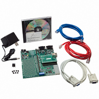
KIT DEVELOP NETWORK FOR MOD5272
Manufacturer
NetBurner Inc
Series
ColdFire®r
Datasheets
1.MOD5272-100IR.pdf
(2 pages)
2.MOD5272-100IR.pdf
(550 pages)
3.NNDK-MOD5282-KIT.pdf
(2 pages)
Specifications of NNDK-MOD5272-KIT
Main Purpose
*
Embedded
*
Utilized Ic / Part
MOD5272
Primary Attributes
*
Secondary Attributes
*
Processor To Be Evaluated
MOD5272
Interface Type
RS-232, RS-485, USB
Lead Free Status / RoHS Status
Contains lead / RoHS non-compliant
Lead Free Status / RoHS Status
Lead free / RoHS Compliant, Contains lead / RoHS non-compliant
Other names
528-1001


PLIC Timing Generator
The clock generator uses a 14-bit counter to divide CLKIN. This limits the reference
clock’s minimum frequency to CLKIN divided by 16,384.
To summarize these two points:
The control of the clock generator block is provided through the PCSR register detailed in
Section 13.5.22, “Clock Select Register (PCSR).”
The process is illustrated by this example. Suppose the following:
The appropriate reference clock is selected by programming PLCLKSEL[CKI1, CKI0],
Section 13.5.22, “Clock Select Register (PCSR).” The multiplication factor is 16
(1.024 MHz / 64 KHz) and is specified by PLCLKSEL[CMULT0-2]. The division ratio
between the synthesized clock (GDCL), 1.024 MHz, and the synthesized frame sync
(Gen_FSC) must be set. (A Gen_FSC of 8 KHz is assumed). This division ratio is selected
by means of FDIV[2-0]. Finally, the clock generation block should be taken out of bypass
by setting PCSR[NBP].
The above settings can be made by a single write of the 16-bit value 0x802B to PCSR.
The following restrictions should be observed when using the clock generator module:
Figure 13-11 and Figure 13-12 show the connectivity and relationship of the timing signals
within the PLIC block.
13.3.2 Super Frame Sync Generation
Figure 13-11 shows the generation of the 2-KHz super frame sync. The choice of either
FSC0 or FSC1 is possible using P1CR[FSM]. This allows either the port 0 or port 1 timing
to be used to generate the 2-KHz super frame sync interrupt. The SFSC block then divides
this accordingly. When P1CR[FSM] is set, FSC1 is the source of the super frame sync. In
case P1CR[MS] is 0 (that is, port 1 is in slave mode), the interrupt is ultimately driven by
an external source. In case the M/S bit is 1 (that is, port 1 is in master mode), FSC1
ultimately comes from port 0.
13-12
• Synthesized clock x 20 < CLKIN
• Reference clock > CLKIN / 16,384
• CPU clock = 66 MHz
• Reference clock = 64 KHz
• Synthesized clock = 1.024 MHz
• The smallest multiplication factor is 2.
• CLKIN should be significantly greater than (> 20 times) the synthesized clock.
MCF5272 User’s Manual
(Recommended)
(Required)
MOTOROLA
Related parts for NNDK-MOD5272-KIT
Image
Part Number
Description
Manufacturer
Datasheet
Request
R

Part Number:
Description:
BOARD SERIAL-ETHERNET 512K FLASH
Manufacturer:
NetBurner Inc
Datasheet:

Part Number:
Description:
PROCESSOR MODULE FLASH MOD5272
Manufacturer:
NetBurner Inc
Datasheet:

Part Number:
Description:
PROCESSOR MODULE 512KB FLASH
Manufacturer:
NetBurner Inc
Datasheet:

Part Number:
Description:
DUAL PORT SERIAL-ETHERNET
Manufacturer:
NetBurner Inc
Datasheet:

Part Number:
Description:
PROCESSOR MODULE FLASH
Manufacturer:
NetBurner Inc
Datasheet:

Part Number:
Description:
PROCESSOR MODULE 512KB FLASH
Manufacturer:
NetBurner Inc
Datasheet:

Part Number:
Description:
MOD5234 10/100 ETHERNET MODULE
Manufacturer:
NetBurner Inc
Datasheet:

Part Number:
Description:
KIT DEVELOP NETWORK FOR MOD5282
Manufacturer:
NetBurner Inc
Datasheet:

Part Number:
Description:
DUAL PORT SERIAL-ETHERNET
Manufacturer:
NetBurner Inc
Datasheet:

Part Number:
Description:
Ethernet Modules & Development Tools 32 Bit 66MHz 40 Pin DIP Industrial Temp
Manufacturer:
NetBurner Inc
Datasheet:

Part Number:
Description:
Ethernet Modules & Development Tools MOD5213 DEVELOPMENT KIT
Manufacturer:
NetBurner Inc

Part Number:
Description:
Ethernet Modules & Development Tools DUAL PORT SERIAL EHTERNET DEVICE
Manufacturer:
NetBurner Inc
Datasheet:

Part Number:
Description:
Ethernet ICs 32bit 147MHz CAN-to- Ethnt Device IndTemp
Manufacturer:
NetBurner Inc
Datasheet: