NNDK-MOD5272-KIT NetBurner Inc, NNDK-MOD5272-KIT Datasheet - Page 124
NNDK-MOD5272-KIT
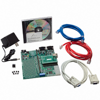
Manufacturer Part Number
NNDK-MOD5272-KIT
Description
KIT DEVELOP NETWORK FOR MOD5272
Manufacturer
NetBurner Inc
Series
ColdFire®r
Datasheets
1.MOD5272-100IR.pdf
(2 pages)
2.MOD5272-100IR.pdf
(550 pages)
3.NNDK-MOD5282-KIT.pdf
(2 pages)
Specifications of NNDK-MOD5272-KIT
Main Purpose
*
Embedded
*
Utilized Ic / Part
MOD5272
Primary Attributes
*
Secondary Attributes
*
Processor To Be Evaluated
MOD5272
Interface Type
RS-232, RS-485, USB
Lead Free Status / RoHS Status
Contains lead / RoHS non-compliant
Lead Free Status / RoHS Status
Lead free / RoHS Compliant, Contains lead / RoHS non-compliant
Other names
528-1001


Signal Description
5.2 Signal Description
Table 5-1 describes debug module signals. All ColdFire debug signals are unidirectional
and related to a rising edge of the processor core’s clock signal. The standard 26-pin debug
connector is shown in Section 5.8, “Motorola-Recommended BDM Pinout.”
Figure 5-2 shows PSTCLK timing with respect to PST and DDATA.
5.3 Real-Time Trace Support
Real-time trace, which defines the dynamic execution path, is a fundamental debug
function. The ColdFire solution is to include a parallel output port providing encoded
processor status and data to an external development system. This port is partitioned into
two 4-bit nibbles: one nibble allows the processor to transmit processor status, (PST), and
the other allows operand data to be displayed (debug data, DDATA). The processor status
Development Serial
Clock (DSCLK)
Development Serial
Input (DSI)
Development Serial
Output (DSO)
Breakpoint (BKPT)
Processor Status
Clock (PSTCLK)
Debug Data
(DDATA[3:0])
Processor Status
(PST[3:0])
5-2
Signal
PST
or
PSTCLK
DDATA
Internally synchronized input. (The logic level on DSCLK is validated if it has the same value on
two consecutive rising CLKIN edges.) Clocks the serial communication port to the debug
module during packet transfers. Maximum frequency is 1/5 the processor status clock
(PSTCLK) speed. At the synchronized rising edge of DSCLK, the data input on DSI is sampled
and DSO changes state.
Internally synchronized input that provides data input for the serial communication port to the
debug module.
Provides serial output communication for debug module responses. DSO is registered
internally.
state after the current instruction completes. Halt status is reflected on processor status signals
(PST[3:0]) as the value 0xF.
Delayed version of the processor clock. Its rising edge appears in the center of valid PST and
DDATA output. See Figure 5-2. PSTCLK indicates when the development system should
sample PST and DDATA values.
These output signals display the register breakpoint status as a default, or optionally, captured
address and operand values. The capturing of data values is controlled by the setting of the
CSR. Additionally, execution of the WDDATA instruction by the processor captures operands
which are displayed on DDATA. These signals are updated each processor cycle.
These output signals report the processor status. Table 5-2 shows the encoding of these
signals. These outputs indicate the current status of the processor pipeline and, as a result, are
not related to the current bus transfer. The PST value is updated each processor cycle.
Input used to request a manual breakpoint. Assertion of BKPT puts the processor into a halted
Table 5-1. Debug Module Signals
Figure 5-2. PSTCLK Timing
MCF5272 User’s Manual
Description
MOTOROLA
Related parts for NNDK-MOD5272-KIT
Image
Part Number
Description
Manufacturer
Datasheet
Request
R

Part Number:
Description:
BOARD SERIAL-ETHERNET 512K FLASH
Manufacturer:
NetBurner Inc
Datasheet:

Part Number:
Description:
PROCESSOR MODULE FLASH MOD5272
Manufacturer:
NetBurner Inc
Datasheet:

Part Number:
Description:
PROCESSOR MODULE 512KB FLASH
Manufacturer:
NetBurner Inc
Datasheet:

Part Number:
Description:
DUAL PORT SERIAL-ETHERNET
Manufacturer:
NetBurner Inc
Datasheet:

Part Number:
Description:
PROCESSOR MODULE FLASH
Manufacturer:
NetBurner Inc
Datasheet:

Part Number:
Description:
PROCESSOR MODULE 512KB FLASH
Manufacturer:
NetBurner Inc
Datasheet:

Part Number:
Description:
MOD5234 10/100 ETHERNET MODULE
Manufacturer:
NetBurner Inc
Datasheet:

Part Number:
Description:
KIT DEVELOP NETWORK FOR MOD5282
Manufacturer:
NetBurner Inc
Datasheet:

Part Number:
Description:
DUAL PORT SERIAL-ETHERNET
Manufacturer:
NetBurner Inc
Datasheet:

Part Number:
Description:
Ethernet Modules & Development Tools 32 Bit 66MHz 40 Pin DIP Industrial Temp
Manufacturer:
NetBurner Inc
Datasheet:

Part Number:
Description:
Ethernet Modules & Development Tools MOD5213 DEVELOPMENT KIT
Manufacturer:
NetBurner Inc

Part Number:
Description:
Ethernet Modules & Development Tools DUAL PORT SERIAL EHTERNET DEVICE
Manufacturer:
NetBurner Inc
Datasheet:

Part Number:
Description:
Ethernet ICs 32bit 147MHz CAN-to- Ethnt Device IndTemp
Manufacturer:
NetBurner Inc
Datasheet: