NNDK-MOD5272-KIT NetBurner Inc, NNDK-MOD5272-KIT Datasheet - Page 328
NNDK-MOD5272-KIT
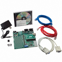
Manufacturer Part Number
NNDK-MOD5272-KIT
Description
KIT DEVELOP NETWORK FOR MOD5272
Manufacturer
NetBurner Inc
Series
ColdFire®r
Datasheets
1.MOD5272-100IR.pdf
(2 pages)
2.MOD5272-100IR.pdf
(550 pages)
3.NNDK-MOD5282-KIT.pdf
(2 pages)
Specifications of NNDK-MOD5272-KIT
Main Purpose
*
Embedded
*
Utilized Ic / Part
MOD5272
Primary Attributes
*
Secondary Attributes
*
Processor To Be Evaluated
MOD5272
Interface Type
RS-232, RS-485, USB
Lead Free Status / RoHS Status
Contains lead / RoHS non-compliant
Lead Free Status / RoHS Status
Lead free / RoHS Compliant, Contains lead / RoHS non-compliant
Other names
528-1001


PLIC Registers
13.5.21 Sync Delay Registers (P0SDR–P3SDR)
All bits in these registers are read/write and are cleared on hardware or software reset.
The PnSDR registers contain the frame sync delay bits for each of the four ports on the
MCF5272.
13.5.22 Clock Select Register (PCSR)
All bits in this register are read/write and are cleared on hardware or software reset.
PCSR controls the PLIC clock generation block. Please refer to Section 13.3, “PLIC
Timing Generator,” for certain restrictions on the use of the clock generation block.
13-32
15–14
13–10
Reset
Bits
9–0
Field FSW1 FSW0
Addr
R/W
FSW[1–0]
15
Name
SD
—
If a sync delay value of 0 is specified, that is,
PnSDR[SD] = 0x000, then the programmable delay block is
transparent. When bypassed, the input frame sync passes
directly to the output, making the frame-sync-width function
defined by PnSDR[FSW] unavailable.
The 8-bit frame-sync-width should not be confused with long
frame sync mode. The PLIC only supports short frame sync in
IDL8 and IDL10 bit modes for interfacing to external
transceivers.
14
Figure 13-33. Sync Delay Registers (P0SDR–P3SDR)
Frame sync width. Sets the width, in clock cycles, of the output frame sync pulse.
00 Frame sync width = 1
01 Frame sync width = 2
10 Frame sync width = 8
11 Frame sync width = 16
Reserved, should be cleared.
Sync delay. Range: 0–1023. Sets the delay, in DCL clock cycles, for DFSC3–DFSC0. The
delay period should be doubled in GCI mode because GCI has two clock cycles per data bit.
See Section 13.3, “PLIC Timing Generator,” for further information.
MBAR + 0x394 (P0SDR); 0x396 (P1SDR); 0x398 (P2SDR); 0x39A (P3SDR)
Table 13-16. P0SDR–P3SDR Field Descriptions
13
—
MCF5272 User’s Manual
10
0000_0000_0000_0000
9
NOTE:
Read/Write
Description
SD
MOTOROLA
0
Related parts for NNDK-MOD5272-KIT
Image
Part Number
Description
Manufacturer
Datasheet
Request
R

Part Number:
Description:
BOARD SERIAL-ETHERNET 512K FLASH
Manufacturer:
NetBurner Inc
Datasheet:

Part Number:
Description:
PROCESSOR MODULE FLASH MOD5272
Manufacturer:
NetBurner Inc
Datasheet:

Part Number:
Description:
PROCESSOR MODULE 512KB FLASH
Manufacturer:
NetBurner Inc
Datasheet:

Part Number:
Description:
DUAL PORT SERIAL-ETHERNET
Manufacturer:
NetBurner Inc
Datasheet:

Part Number:
Description:
PROCESSOR MODULE FLASH
Manufacturer:
NetBurner Inc
Datasheet:

Part Number:
Description:
PROCESSOR MODULE 512KB FLASH
Manufacturer:
NetBurner Inc
Datasheet:

Part Number:
Description:
MOD5234 10/100 ETHERNET MODULE
Manufacturer:
NetBurner Inc
Datasheet:

Part Number:
Description:
KIT DEVELOP NETWORK FOR MOD5282
Manufacturer:
NetBurner Inc
Datasheet:

Part Number:
Description:
DUAL PORT SERIAL-ETHERNET
Manufacturer:
NetBurner Inc
Datasheet:

Part Number:
Description:
Ethernet Modules & Development Tools 32 Bit 66MHz 40 Pin DIP Industrial Temp
Manufacturer:
NetBurner Inc
Datasheet:

Part Number:
Description:
Ethernet Modules & Development Tools MOD5213 DEVELOPMENT KIT
Manufacturer:
NetBurner Inc

Part Number:
Description:
Ethernet Modules & Development Tools DUAL PORT SERIAL EHTERNET DEVICE
Manufacturer:
NetBurner Inc
Datasheet:

Part Number:
Description:
Ethernet ICs 32bit 147MHz CAN-to- Ethnt Device IndTemp
Manufacturer:
NetBurner Inc
Datasheet: