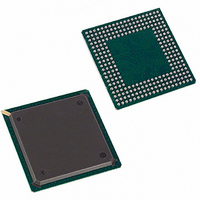
DS31256 Maxim Integrated Products, DS31256 Datasheet - Page 82

DS31256
Manufacturer Part Number
DS31256
Description
IC CTRLR HDLC 256-CHANNEL 256BGA
Manufacturer
Maxim Integrated Products
Datasheet
1.DS31256.pdf
(183 pages)
Specifications of DS31256
Controller Type
HDLC Controller
Interface
Serial
Voltage - Supply
3 V ~ 3.6 V
Current - Supply
500mA
Operating Temperature
0°C ~ 70°C
Mounting Type
Surface Mount
Package / Case
256-BGA
Lead Free Status / RoHS Status
Contains lead / RoHS non-compliant
Available stocks
Company
Part Number
Manufacturer
Quantity
Price
Part Number:
DS31256
Manufacturer:
DALLAS
Quantity:
20 000
Bit #
Name
Default
Bit #
Name
Default
Bit 14/Indirect Access Read/Write (IARW). When the host wishes to read data from the internal transmit low-
watermark RAM, this bit should be written to 1 by the host. This causes the device to begin obtaining the data
from the channel location indicated by the HCID bits. During the read access, the IAB bit is set to 1. Once the data
is ready to be read from the TFLWM register, the IAB bit is set to 0. When the host wishes to write data to the
internal transmit low-watermark RAM, this bit should be written to 0 by the host. This causes the device to take
the data that is currently present in the TFLWM register and write it to the channel location indicated by the HCID
bits. When the device has completed the write, the IAB is set to 0.
Bit 15/Indirect Access Busy (IAB). When an indirect read or write access is in progress, this read-only bit is set
to 1. During a read operation, this bit is set to 1 until the data is ready to be read. It is set to 0 when the data is
ready to be read. During a write operation, this bit is set to 1 while the write is taking place. It is set to 0 once the
write operation has completed.
Register Name:
Register Description:
Register Address:
Note: Bits that are underlined are read-only; all other bits are read-write.
Bits 0 to 9/Low Watermark (TLWM0 to TLWM9). These bits indicate the setting of the transmit low
watermark. The low watermark setting is the number of blocks left in the transmit FIFO before the DMA gets
more data from the PCI bus. The low-watermark setting must be between (inclusive) one block and one less than
the number of blocks in the link-list chain for the particular channel involved. For example, if five blocks are
linked together, the low watermark can be set to 1, 2, or 3. In other words, the low watermark can be set at a value
of 1 to N - 2, where N = number of block linked together. Any other numbers are illegal.
0000000000 (000h) = invalid setting
0000000001 (001h) = low watermark is 1 block
0000000010 (002h) = low watermark is 2 blocks
0111111111 (1FFh) = low watermark is 511 blocks
1111111111 (3FFh) = low watermark is 1023 blocks
TLWM7
n/a
15
7
TFLWM
Transmit FIFO Low Watermark
09A4h
TLWM6
n/a
14
6
TLWM5
n/a
13
5
TLWM4
n/a
12
82 of 183
4
TLWM3
n/a
11
3
TLWM2
n/a
10
2
TLWM1
TLWM9
1
9
TLWM0
TLWM8
0
8


