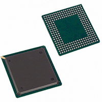
DS31256 Maxim Integrated Products, DS31256 Datasheet - Page 167

DS31256
Manufacturer Part Number
DS31256
Description
IC CTRLR HDLC 256-CHANNEL 256BGA
Manufacturer
Maxim Integrated Products
Datasheet
1.DS31256.pdf
(183 pages)
Specifications of DS31256
Controller Type
HDLC Controller
Interface
Serial
Voltage - Supply
3 V ~ 3.6 V
Current - Supply
500mA
Operating Temperature
0°C ~ 70°C
Mounting Type
Surface Mount
Package / Case
256-BGA
Lead Free Status / RoHS Status
Contains lead / RoHS non-compliant
Available stocks
Company
Part Number
Manufacturer
Quantity
Price
Part Number:
DS31256
Manufacturer:
DALLAS
Quantity:
20 000
DS31256 256-Channel, High-Throughput HDLC Controller
BYPASS. When the BYPASS instruction is latched into the parallel instruction register, JTDI connects
to JTDO through the 1-bit bypass test register. This allows data to pass from JTDI to JTDO without
affecting the device’s normal operation.
IDCODE. When the IDCODE instruction is latched into the parallel instruction register, the
identification test register is selected. The device identification code loads into the identification register
on the rising edge of JTCLK following entry into the Capture-DR state. Shift-DR can be used to shift the
identification code out serially through JTDO. During Test-Logic-Reset, the identification code is forced
into the instruction register’s parallel output. The device ID code always has 1 in the LSB position. The
next 11 bits identify the manufacturer’s JEDEC number and number of continuation bytes followed by 16
bits for the device and 4 bits for the version. The device ID code for the DS31256 is 00006143h.
12.4 Test Registers
IEEE 1149.1 requires a minimum of two test registers—the bypass register and the boundary scan
register. An optional identification register has been included in the DS31256 design that is used in
conjunction with the IDCODE instruction and the Test-Logic-Reset state of the TAP controller.
Bypass Register
This is a single 1-bit shift register used in conjunction with the BYPASS, CLAMP, and HIGHZ
instructions that provides a short path between JTDI and JTDO.
Boundary Scan Register
This register contains both a shift register path and a latched parallel output for all control cells and digital
I/O cells. Visit
www.maxim-ic.com/telecom
for a downloadable BDSL file that contains all bit identity
and definition information.
Identification Register
The identification register contains a 32-bit shift register and a 32-bit latched parallel output. This register
is selected during the IDCODE instruction and when the TAP controller is in the Test-Logic-Reset state.
167 of 183


