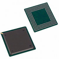
DS31256 Maxim Integrated Products, DS31256 Datasheet - Page 153

DS31256
Manufacturer Part Number
DS31256
Description
IC CTRLR HDLC 256-CHANNEL 256BGA
Manufacturer
Maxim Integrated Products
Datasheet
1.DS31256.pdf
(183 pages)
Specifications of DS31256
Controller Type
HDLC Controller
Interface
Serial
Voltage - Supply
3 V ~ 3.6 V
Current - Supply
500mA
Operating Temperature
0°C ~ 70°C
Mounting Type
Surface Mount
Package / Case
256-BGA
Lead Free Status / RoHS Status
Contains lead / RoHS non-compliant
Available stocks
Company
Part Number
Manufacturer
Quantity
Price
Part Number:
DS31256
Manufacturer:
DALLAS
Quantity:
20 000
Bit #
Name
Default
Bit #
Name
Default
11.2 Local Bus Bridge Mode Control Register Description
Register Name:
Register Description:
Register Address:
Note: This register can only be accessed through the PCI bus and therefore only in the PCI bridge mode. In configuration mode, this register
cannot be accessed. It is set to all zeros upon a hardware reset issued through the PRST pin. It is not affected by a software reset issued
through the RST control bit in the master reset and ID (MRID) register.
Note: Bits that are underlined are read-only; all other bits are read-write.
Bit 0/Local Bus Clock Enable (LCLKE)
Bit 1/Local Bus Arbitration Enable (LARBE). When enabled, the LHOLD (LBR), LBGACK, and LHLDA
(LBG) signal pins are active and the proper arbitration handshake sequence must occur for a proper bus
transaction. When disabled, the LHOLD (LBR), LBGACK, and LHLDA (LBG) signal pins are deactivated and
bus arbitration on the local bus is not invoked. Also, the arbitration timer is enabled (see the description of the
LAT0 to LAT3 bits) when LARBE is set to 1.
Bit 2/Local Bus Ready Control Bit 0 (LRDY0). LSB
Bit 3/Local Bus Ready Control Bit 1 (LRDY1)
Bit 4/Local Bus Ready Control Bit 2 (LRDY2)
Bit 5/Local Bus Ready Control Bit 3 (LRDY3). MSB. These control bits determine the duration of the local bus
transaction in the PCI bridge mode. The bus transaction can either be controlled through the external LRDY input
signal or through a predetermined period of 1 to 11 LCLK periods.
0 = tri-state the LCLK output signal pin
1 = allow LCLK to appear at the pin
0 = local bus arbitration is disabled
1 = local bus arbitration is enabled
0000 = use the LRDY signal input pin to control the bus transaction
0001 = bus transaction is defined as 1 LCLK period
0010 = bus transaction is defined as 2 LCLK periods
0011 = bus transaction is defined as 3 LCLK periods
0100 = bus transaction is defined as 4 LCLK periods
0101 = bus transaction is defined as 5 LCLK periods
0110 = bus transaction is defined as 6 LCLK periods
0111 = bus transaction is defined as 7 LCLK periods
1000 = bus transaction is defined as 8 LCLK periods
1001 = bus transaction is defined as 9 LCLK periods
1010 = bus transaction is defined as 10 LCLK periods
1011 = bus transaction is defined as 11 LCLK periods
1100 = illegal state
1101 = illegal state
1110 = illegal state
1111 = illegal state
n/a
n/a
15
7
0
0
LBBMC
Local Bus Bridge Mode Control
0040h
LBW
n/a
14
6
0
0
LRDY3
n/a
13
5
0
0
LRDY2
153 of 183
n/a
12
4
0
0
LRDY1
LAT3
11
3
0
0
LRDY0
LAT2
10
2
0
0
LARBE
LAT1
1
0
9
0
LCLKE
LAT0
0
0
8
0


