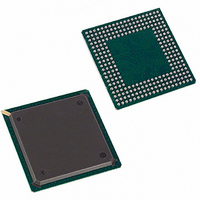
DS31256 Maxim Integrated Products, DS31256 Datasheet - Page 50

DS31256
Manufacturer Part Number
DS31256
Description
IC CTRLR HDLC 256-CHANNEL 256BGA
Manufacturer
Maxim Integrated Products
Datasheet
1.DS31256.pdf
(183 pages)
Specifications of DS31256
Controller Type
HDLC Controller
Interface
Serial
Voltage - Supply
3 V ~ 3.6 V
Current - Supply
500mA
Operating Temperature
0°C ~ 70°C
Mounting Type
Surface Mount
Package / Case
256-BGA
Lead Free Status / RoHS Status
Contains lead / RoHS non-compliant
Available stocks
Company
Part Number
Manufacturer
Quantity
Price
Part Number:
DS31256
Manufacturer:
DALLAS
Quantity:
20 000
Bit 0/Invert Clock Enable (TICE)
Bit 1/Invert Data Enable (TIDE)
Bit 2/Invert Sync Enable (TISE)
Bit 3/Force Data All Ones (TFDA1)
Bit 4/Sync Delay Bit 0 (TSD0); Bit 5/Sync Delay Bit 1 (TSD1). These bits define the format of the sync signal
that is applied to the TS[n] input. These bits are ignored if the port has been configured to operate in an
unchannelized fashion (TUEN = 1).
Bit 6/Sync Select Bit 0 (TSS0); Bit 7/Sync Select Bit 1 (TSS1). These bits select the mode in which each port
operates. Each port can be configured to accept 24, 32, 64, or 128 DS0 channels at an 8kHz rate. These bits are
ignored if the port has been configured to operate in an unchannelized fashion (TUEN = 1).
Bit 8/Port 0 High-Speed Mode (TP0 (1, 2) HS). If enabled, the port 0 (1 or 2) Layer 1 state machine logic is
defeated and TC0 (1, 2) and TD0 (1, 2) are routed to some dedicated high-speed HDLC processing logic. Only
present in TP0CR, TP1CR, and TP2CR. Bit 8 is not assigned in ports 3 through 15.
Bit 9/Unchannelized Enable (TUEN). When enabled, this bit forces the port to operate in an unchannelized
fashion. When disabled, the port operates in a channelized mode. This bit overrides the transmit channel-enable
(TCHEN) bit in the transmit Layer 1 configuration (T[n]CFG[j]) registers, which are described in Section 6.3.
Bit 10/Unchannelized Network Loopback Enable (UNLB). See
used for ports 0 and 1 when they are operating at speeds greater than 10MHz.
Bit 11/Unchannelized BERT Select (TUBS). This bit is ignored if TUEN = 0. This bit overrides the transmit
BERT (TBERT) bit in the transmit layer 1 configuration (T[n]CFG[j]) registers, which are described in
Section 6.3.
0 = do not invert clock (normal mode)
1 = invert clock (inverted mode)
0 = do not invert data (normal mode)
1 = invert data (inverted mode)
0 = do not invert sync (normal mode)
1 = invert sync pulse (inverted mode)
0 = force all data at TD to be 1
1 = allow data to be transmitted normally
00 = sync pulse is 0 clocks early
01 = sync pulse is 1/2 clock early
10 = sync pulse is 1 clock early
11 = sync pulse is 2 clocks early
00 = T1 Mode (24 DS0 channels and 193 RC clocks between TS sync signals)
01 = E1 Mode (32 DS0 channels and 256 RC clocks between TS sync signals)
10 = 4.096MHz Mode (64 DS0 channels and 512 RC clocks between TS sync signals)
11 = 8.192MHz Mode (128 DS0 channels and 1024 RC clocks between TS sync signals)
0 = disabled
1 = enabled
0 = channelized mode
1 = unchannelized mode
0 = loopback disabled
1 = loopback enabled
0 = source transmit data from the HDLC controller
1 = source transmit data from the BERT block
50 of 183
Figure 6-1
for details. This loopback cannot be


