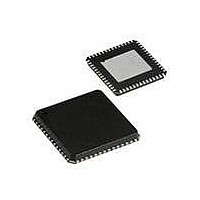
CYRF69213-40LFXC Cypress Semiconductor Corp, CYRF69213-40LFXC Datasheet - Page 8

CYRF69213-40LFXC
Manufacturer Part Number
CYRF69213-40LFXC
Description
IC PROC 8K FLASH 40VQFN
Manufacturer
Cypress Semiconductor Corp
Series
CYRFr
Type
Transceiverr
Datasheet
1.CYRF69213-40LFXC.pdf
(77 pages)
Specifications of CYRF69213-40LFXC
Package / Case
40-VQFN Exposed Pad, 40-HVQFN, 40-SQFN, 40-DHVQFN
Frequency
2.4GHz
Data Rate - Maximum
1Mbps
Modulation Or Protocol
ISM
Applications
General Purpose
Power - Output
4dBm
Sensitivity
-97dBm
Voltage - Supply
4 V ~ 5.5 V
Current - Receiving
23.4mA
Current - Transmitting
36.6mA
Data Interface
PCB, Surface Mount
Memory Size
8kB Flash, 256B SRAM
Antenna Connector
PCB, Surface Mount
Operating Temperature
0°C ~ 70°C
Operating Frequency
2497 MHz
Operating Supply Voltage
2.5 V or 3.3 V
Maximum Operating Temperature
+ 70 C
Minimum Operating Temperature
0 C
Mounting Style
SMD/SMT
Operating Temperature (min)
0C
Operating Temperature (max)
70C
Operating Temperature Classification
Commercial
Operating Supply Voltage (min)
1.8V
Operating Supply Voltage (typ)
2.5/3.3V
Operating Supply Voltage (max)
3.6V
Lead Free Status / RoHS Status
Lead free / RoHS Compliant
For Use With
770-1001 - ISP 4PORT CYPRESS ENCORE II MCU
Lead Free Status / Rohs Status
Lead free / RoHS Compliant
Other names
428-1934
Available stocks
Company
Part Number
Manufacturer
Quantity
Price
Part Number:
CYRF69213-40LFXC
Manufacturer:
CYPRESS/赛普拉斯
Quantity:
20 000
Following are the requirements for the crystal to be directly
connected to XTAL pin and GND:
■
■
■
■
■
■
■
The MCU function features an internal oscillator. With the
presence of USB traffic, the internal oscillator can be set to
precisely tune to USB timing requirements (24 MHz ±1.5%). The
clock generator provides the 12 MHz and 24 MHz clocks that
remain internal to the microcontroller.
GPIO Interface
The MCU function features up to 20 general purpose I/O (GPIO)
pins to support USB, PS/2, and other applications. The I/O pins
are grouped into five ports (Port 0 to 4). The pins on Port 0 and
Port 1 may each be configured individually while the pins on
Ports 2, 3, and 4 may only be configured as a group. Each GPIO
port supports high impedance inputs, configurable pull up, open
drain output, CMOS/TTL inputs, and CMOS output with up to five
pins that support programmable drive strength of up to 50 mA
sink current. GPIO Port 1 features four pins that interface at a
voltage level of 3.3 volts. Additionally, each I/O pin can be used
to generate a GPIO interrupt to the microcontroller. Each GPIO
port has its own GPIO interrupt vector with the exception of GPIO
Port 0. GPIO Port 0 has three dedicated pins that have
independent interrupt vectors (P0.3–P0.4).
Power On Reset/Low Voltage Detect
The power on reset circuit detects logic when power is applied
to the device, resets the logic to a known state, and begins
executing instructions at Flash address 0x0000. When power
falls below a programmable trip voltage, it generates reset or
may be configured to generate interrupt. There is a low voltage
detect circuit that detects when V
mable trip voltage. It may be configurable to generate an LVD
interrupt to inform the processor about the low voltage event.
POR and LVD share the same interrupt. There is not a separate
interrupt for each. The Watchdog timer can be used to ensure
the firmware never gets stalled in an infinite loop.
Power Management
The device draws its power supply from the USB V
V
3.3 V regulator. This 3.3 V is supplied to the radio function via
P1.2/V
Document #: 001-07552 Rev. *D
bus
Nominal Frequency: 12 MHz
Operating Mode: Fundamental Mode
Resonance Mode: Parallel Resonant
Frequency Stability: ±30 ppm
Series Resistance: <60 ohms
Load Capacitance: 10 pF
Drive Level:100 μ W
supplies power to the MCU function, which has an internal
REG
after proper filtering as shown in Figure 3.
CC
drops below a program-
bus
line. The
Figure 3. Power Management From Internal Regulator
Timers
The free-running 16-bit timer provides two interrupt sources: the
programmable interval timer with 1 μ s resolution and the
1.024 ms outputs. The timer can be used to measure the
duration of an event under firmware control by reading the timer
at the start and at the end of an event, then calculating the
difference between the two values.
USB Interface
The MCU function includes an integrated USB serial interface
engine (SIE) that allows the chip to easily interface to a USB
host. The hardware supports one USB device address with three
endpoints.
Low Noise Amplifier (LNA) and Received
Signal Strength Indication (RSSI)
The gain of the receiver may be controlled directly by clearing
the AGC EN bit and writing to the Low Noise Amplifier (LNA) bit
of the RX_CFG_ADR register. When the LNA bit is cleared, the
receiver gain is reduced by approximately 20 dB, allowing
accurate reception of very strong received signals (for example
when operating a receiver very close to the transmitter). An
additional 20 dB of receiver attenuation can be added by setting
the Attenuation (ATT) bit; this allows data reception to be limited
to devices at very short ranges. Disabling AGC and enabling
LNA is recommended unless receiving from a device using
external PA.
The RSSI register returns the relative signal strength of the
on-channel signal power.
When receiving, the device may be configured to automatically
measure and store the relative strength of the signal being
received as a 5-bit value. When enabled, an RSSI reading is
0.1µF
V
DD
0.047µF
P1.2 / V
V
DD_MICRO
1 ohm
0.047µF
Reg
0.047µF
PRoC LP
0.047µF
0.047µF
CYRF69213
0.047µF
0.047µF
Page 8 of 77
0.047µF
[+] Feedback


