CYRF69213-40LFXC Cypress Semiconductor Corp, CYRF69213-40LFXC Datasheet - Page 41
CYRF69213-40LFXC
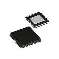
Manufacturer Part Number
CYRF69213-40LFXC
Description
IC PROC 8K FLASH 40VQFN
Manufacturer
Cypress Semiconductor Corp
Series
CYRFr
Type
Transceiverr
Datasheet
1.CYRF69213-40LFXC.pdf
(77 pages)
Specifications of CYRF69213-40LFXC
Package / Case
40-VQFN Exposed Pad, 40-HVQFN, 40-SQFN, 40-DHVQFN
Frequency
2.4GHz
Data Rate - Maximum
1Mbps
Modulation Or Protocol
ISM
Applications
General Purpose
Power - Output
4dBm
Sensitivity
-97dBm
Voltage - Supply
4 V ~ 5.5 V
Current - Receiving
23.4mA
Current - Transmitting
36.6mA
Data Interface
PCB, Surface Mount
Memory Size
8kB Flash, 256B SRAM
Antenna Connector
PCB, Surface Mount
Operating Temperature
0°C ~ 70°C
Operating Frequency
2497 MHz
Operating Supply Voltage
2.5 V or 3.3 V
Maximum Operating Temperature
+ 70 C
Minimum Operating Temperature
0 C
Mounting Style
SMD/SMT
Operating Temperature (min)
0C
Operating Temperature (max)
70C
Operating Temperature Classification
Commercial
Operating Supply Voltage (min)
1.8V
Operating Supply Voltage (typ)
2.5/3.3V
Operating Supply Voltage (max)
3.6V
Lead Free Status / RoHS Status
Lead free / RoHS Compliant
For Use With
770-1001 - ISP 4PORT CYPRESS ENCORE II MCU
Lead Free Status / Rohs Status
Lead free / RoHS Compliant
Other names
428-1934
Available stocks
Company
Part Number
Manufacturer
Quantity
Price

Part Number:
CYRF69213-40LFXC
Manufacturer:
CYPRESS/赛普拉斯
Quantity:
20 000


Table 55. P1.3 Configuration (P13CR) [0x10] [R/W]
Table 56. P1.4–P1.6 Configuration (P14CR–P16CR) [0x11–0x13] [R/W]
Table 57. P1.7 Configuration (P17CR) [0x14] [R/W]
Document #: 001-07552 Rev. *D
Bit #
Field
Read/Write
Default
This register controls the operation of the P1.3 pin. This register exists in all CYRF69213 parts
The P1.3 GPIO’s threshold is always set to TTL
When the SPI hardware is enabled, the output enable and output state of the pin is controlled by the SPI circuitry. When the SPI
hardware is disabled, the pin is controlled by the Output Enable bit and the corresponding bit in the P1 data register
Regardless of whether the pin is used as an SPI or GPIO pin the Int Enable, Int act Low, 3.3V Drive, High Sink, Open Drain, and
Pull up Enable control the behavior of the pin
The 50 mA sink drive capability is only available in the CY7C638xx.
Bit #
Field
Read/Write
Default
T
The P1.4–P1.6 GPIO’s threshold is always set to TTL
When the SPI hardware is enabled, pins that are configured as SPI Use have their output enable and output state controlled by
the SPI circuitry. When the SPI hardware is disabled or a pin has its SPI Use bit clear, the pin is controlled by the Output Enable
bit and the corresponding bit in the P1 data register
Regardless of whether any pin is used as an SPI or GPIO pin the Int Enable, Int act Low, 3.3V Drive, High Sink, Open Drain,
and Pull up Enable control the behavior of the pin
Bit 7
Important Note for Comm Modes 01 or 10 (SPI Master or SPI Slave, see
When configured for SPI (SPI Use = 1 and Comm Modes [1:0] = SPI Master or SPI Slave mode), the input/output direction of
pins P1.3, P1.5, and P1.6 is set automatically by the SPI logic. However, pin P1.4's input/output direction is NOT automatically
set; it must be explicitly set by firmware. For SPI Master mode, pin P1.4 must be configured as an output; for SPI Slave mode,
pin P1.4 must be configured as an input
Bit #
Field
Read/Write
Default
T
The 50 mA sink drive capability is only available in the CY7C638xx. The P1.7 GPIO’s threshold is always set to TTL
hese registers control the operation of pins P1.4–P1.6, respectively
his register controls the operation of pin P1.7. This register only exists in CY7C638xx
SPI Use
0 = Disable the SPI alternate function. The pin is used as a GPIO
1 = Enable the SPI function. The SPI circuitry controls the output of the pin
Reserved
Reserved
SPI Use
R/W
7
–
0
7
–
0
7
0
Int Enable
Int Enable
Int Enable
R/W
R/W
R/W
6
0
6
0
6
0
Int Act Low
Int Act Low
Int Act Low
R/W
R/W
R/W
5
0
5
0
5
0
TTL Thresh
3.3V Drive
3.3V Drive
R/W
4
0
R/W
R/W
4
0
4
0
High Sink
High Sink
High Sink
R/W
3
0
R/W
R/W
3
0
3
0
Table 60
Open Drain Pull up Enable Output Enable
)
Open Drain
Open Drain
R/W
2
0
R/W
R/W
2
0
2
0
Pull up En-
Pull up En-
R/W
1
0
able
R/W
able
R/W
1
0
1
0
CYRF69213
Output En-
Output En-
Page 41 of 77
able
R/W
able
R/W
R/W
0
0
0
0
0
0
[+] Feedback
Related parts for CYRF69213-40LFXC
Image
Part Number
Description
Manufacturer
Datasheet
Request
R

Part Number:
Description:
Manufacturer:
Cypress Semiconductor Corp
Datasheet:
Part Number:
Description:
Manufacturer:
Cypress Semiconductor Corp
Datasheet:
Part Number:
Description:
Manufacturer:
Cypress Semiconductor Corp
Datasheet:
Part Number:
Description:
Manufacturer:
Cypress Semiconductor Corp
Datasheet:
Part Number:
Description:
Manufacturer:
Cypress Semiconductor Corp
Datasheet: