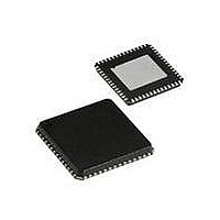
CYRF69213-40LFXC Cypress Semiconductor Corp, CYRF69213-40LFXC Datasheet - Page 33

CYRF69213-40LFXC
Manufacturer Part Number
CYRF69213-40LFXC
Description
IC PROC 8K FLASH 40VQFN
Manufacturer
Cypress Semiconductor Corp
Series
CYRFr
Type
Transceiverr
Datasheet
1.CYRF69213-40LFXC.pdf
(77 pages)
Specifications of CYRF69213-40LFXC
Package / Case
40-VQFN Exposed Pad, 40-HVQFN, 40-SQFN, 40-DHVQFN
Frequency
2.4GHz
Data Rate - Maximum
1Mbps
Modulation Or Protocol
ISM
Applications
General Purpose
Power - Output
4dBm
Sensitivity
-97dBm
Voltage - Supply
4 V ~ 5.5 V
Current - Receiving
23.4mA
Current - Transmitting
36.6mA
Data Interface
PCB, Surface Mount
Memory Size
8kB Flash, 256B SRAM
Antenna Connector
PCB, Surface Mount
Operating Temperature
0°C ~ 70°C
Operating Frequency
2497 MHz
Operating Supply Voltage
2.5 V or 3.3 V
Maximum Operating Temperature
+ 70 C
Minimum Operating Temperature
0 C
Mounting Style
SMD/SMT
Operating Temperature (min)
0C
Operating Temperature (max)
70C
Operating Temperature Classification
Commercial
Operating Supply Voltage (min)
1.8V
Operating Supply Voltage (typ)
2.5/3.3V
Operating Supply Voltage (max)
3.6V
Lead Free Status / RoHS Status
Lead free / RoHS Compliant
For Use With
770-1001 - ISP 4PORT CYPRESS ENCORE II MCU
Lead Free Status / Rohs Status
Lead free / RoHS Compliant
Other names
428-1934
Available stocks
Company
Part Number
Manufacturer
Quantity
Price
Part Number:
CYRF69213-40LFXC
Manufacturer:
CYPRESS/赛普拉斯
Quantity:
20 000
Wakeup Sequence
When asleep, the only event that can wake the system up is an
interrupt. The global interrupt enable of the CPU flag register
does not need to be set. Any unmasked interrupt wakes the
system up. It is optional for the CPU to actually take the interrupt
after the wakeup sequence. The wakeup sequence is synchro-
nized to the 32 kHz clock for purposes of sequencing a startup
delay, to allow the Flash memory module enough time to power
up before the CPU asserts the first read access. Another reason
for the delay is to allow the oscillator, Bandgap, and LVD/POR
circuits time to settle before actually being used in the system.
As shown in
Document #: 001-07552 Rev. *D
2. Due to the specific timing of the register write, the CPU issues
3. The system-wide PD (power down) signal controls several
1. The wakeup interrupt occurs and is synchronized by the neg-
2. At the following positive edge of the 32 kHz clock, the
3. At the following positive edge of the 32 kHz clock, the current
a Bus Request Acknowledge (BRA) on the following positive
edge of the CPU clock. The sleep logic waits for the following
negative edge of the CPU clock and then asserts a
system-wide Power Down (PD) signal. In
is halted and the system-wide power down signal is asserted.
major circuit blocks: The Flash memory module, the internal
24 MHz oscillator, the EFTB filter and the bandgap voltage
reference. These circuits transition into a zero power state.
The only operational circuits on chip are the Low Power oscil-
ative edge of the 32 kHz clock.
system-wide PD signal is negated. The Flash memory
module, internal oscillator, EFTB, and bandgap circuit are all
powered up to a normal operating state.
values for the precision POR and LVD have settled and are
sampled.
Figure
13, the wakeup sequence is as follows:
Firmware write to SCR
SLEEP bit causes an
immediate BRQ
CPUCLK
SLEEP
BRQ
BRA
IOW
PD
Figure 12
CPUCLK edge
CPU captures
BRQ on next
Figure 12. Sleep Timing
the CPU
Note To achieve the lowest possible power consumption during
suspend/sleep, the following conditions must be observed in
addition to considerations for the sleep timer.
■
■
Low Power in Sleep Mode
The following steps are mandatory before configuring the system
into suspend mode to meet the specifications:
All the other blocks go to the power down mode automatically on
suspend.
with a BRA
4. At the following negative edge of the 32 kHz clock (after about
1. Clear P11CR[0], P10CR[0] - during USB and Non-USB oper-
2. Clear the USB Enable USBCR[7] - during USB mode opera-
3. Set P10CR[1] - during non-USB mode operations
4. To avoid current consumption make sure ITMRCLK,
responds
All GPIOs must be set to outputs and driven low
The USB pins P1.0 and P1.1 should be configured as inputs
with their pull ups enabled.
lator, the bandgap refresh circuit, and the supply voltage
monitor (POR/LVD) circuit.
15 µs nominal), the BRQ signal is negated by the sleep logic
circuit. On the following CPUCLK, BRA is negated by the CPU
and instruction execution resumes. Note that in
fixed function blocks, such as Flash, internal oscillator, EFTB,
and bandgap, have about 15 µs start up. The wakeup times
(interrupt to CPU operational) ranges from 75 µs to 105 µs.
ations
tions
TCPCLK, and USBCLK are not sourced by either low power
32KHz oscillator or 24 MHz crystal-less oscillator.
CPU
The 24/48 MHz system clock
bandgap are powered down
CPUCLK, PD is asserted.
is halted; the Flash and
On the falling edge of
CYRF69213
Page 33 of 77
Figure 13
[+] Feedback


