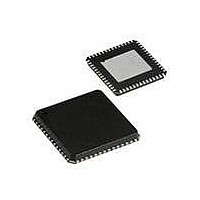
CYRF69213-40LFXC Cypress Semiconductor Corp, CYRF69213-40LFXC Datasheet - Page 27

CYRF69213-40LFXC
Manufacturer Part Number
CYRF69213-40LFXC
Description
IC PROC 8K FLASH 40VQFN
Manufacturer
Cypress Semiconductor Corp
Series
CYRFr
Type
Transceiverr
Datasheet
1.CYRF69213-40LFXC.pdf
(77 pages)
Specifications of CYRF69213-40LFXC
Package / Case
40-VQFN Exposed Pad, 40-HVQFN, 40-SQFN, 40-DHVQFN
Frequency
2.4GHz
Data Rate - Maximum
1Mbps
Modulation Or Protocol
ISM
Applications
General Purpose
Power - Output
4dBm
Sensitivity
-97dBm
Voltage - Supply
4 V ~ 5.5 V
Current - Receiving
23.4mA
Current - Transmitting
36.6mA
Data Interface
PCB, Surface Mount
Memory Size
8kB Flash, 256B SRAM
Antenna Connector
PCB, Surface Mount
Operating Temperature
0°C ~ 70°C
Operating Frequency
2497 MHz
Operating Supply Voltage
2.5 V or 3.3 V
Maximum Operating Temperature
+ 70 C
Minimum Operating Temperature
0 C
Mounting Style
SMD/SMT
Operating Temperature (min)
0C
Operating Temperature (max)
70C
Operating Temperature Classification
Commercial
Operating Supply Voltage (min)
1.8V
Operating Supply Voltage (typ)
2.5/3.3V
Operating Supply Voltage (max)
3.6V
Lead Free Status / RoHS Status
Lead free / RoHS Compliant
For Use With
770-1001 - ISP 4PORT CYPRESS ENCORE II MCU
Lead Free Status / Rohs Status
Lead free / RoHS Compliant
Other names
428-1934
Available stocks
Company
Part Number
Manufacturer
Quantity
Price
Part Number:
CYRF69213-40LFXC
Manufacturer:
CYPRESS/赛普拉斯
Quantity:
20 000
Document #: 001-07552 Rev. *D
Table 37. OSC Control 0 (OSC_CR0) [0x1E0] [R/W]
Bit #
Field
Read/Write
Default
Bits 7:6
Bit 5
Note The periodic Sleep Duty Cycle enabling is independent with the sleep interval shown in the Sleep [1:0] bits below
Bits 4:3
00
01
10
11
Note Sleep intervals are approximate
Bits 2:0
Important Note Correct USB operations require the CPU clock speed be at least 1.5 MHz or not less than USB clock/8. If the two
clocks have the same source then the CPU clock divider should not be set to divide by more than 8. If the two clocks have different
sources, care must be taken to ensure that the maximum ratio of USB Clock/CPU Clock can never exceed 8 across the full specifi-
cation range of both clock sources
Sleep Timer
CPU Speed [2:0]
[1:0]
000
001
010
100
101
011
110
111
Reserved
No Buzz
During sleep (the Sleep bit is set in the CPU_SCR
on periodically to detect any POR and LVD events on the V
to control the duty
the LVD and POR detection circuit to be continuously enabled during sleep. This results in a faster response to an LVD
or POR event during sleep at the expense of a slightly higher than average sleep current
0 = The LVD and POR detection circuit is turned on periodically as configured in the Sleep Duty Cycle
1 = The Sleep Duty Cycle value is overridden. The LVD and POR detection circuit is always enabled
Sleep Timer [1:0]
CPU Speed [2:0]
The CYRF69213 may operate over a range of CPU clock speeds. The reset value for the CPU Speed bits is zero;
therefore, the default CPU speed is one-eighth of the internal 24 MHz, or 3 MHz
Regardless of the CPU Speed bit’s setting, if the actual CPU speed is greater than 12 MHz, the 24 MHz operating
requirements apply. An example of this scenario is a device that is configured to use an external clock, which is sup-
plying a frequency of 20 MHz. If the CPU speed register’s value is 0b011, the CPU clock is 20 MHz. Therefore the sup-
ply voltage requirements for the device are the same as if the part was operating at 24 MHz. The operating voltage
requirements are not relaxed until the CPU speed is at 12 MHz or less
Frequency (Nominal)
512 Hz
64 Hz
8 Hz
1 Hz
Sleep Timer Clock
7
–
0
Reserved
cycle—Table
Oscillator is selected
6
–
0
CPU when Internal
3 MHz (Default)
1.95 ms
15.6 ms
125 ms
1 sec
Sleep Period
R
(Nominal)
1.5 MHz
750 KHz
187 KHz
12 MHz
24 MHz
6 MHz
45). To facilitate the detection of POR and LVD events, the No Buzz bit is used to force
No Buzz
R/W
d
5
0
6 ms
47 ms
375 ms
3 sec
Watchdog Period
(Nominal)
R/W
Sleep Timer [1:0]
Register—Table
4
0
External Clock
CC
Clock In/128
Clock In/16
Clock In/32
Clock In/8
Clock In/4
Clock In/2
Clock In/1
R
pin (the Sleep Duty Cycle bits in the ECO_TR are used
R/W
3
0
41), the LVD and POR detection circuit is turned
d
R/W
2
0
CPU Speed [2:0]
R/W
CYRF69213
1
0
Page 27 of 77
R/W
0
0
[+] Feedback


