CYRF69213-40LFXC Cypress Semiconductor Corp, CYRF69213-40LFXC Datasheet - Page 11
CYRF69213-40LFXC
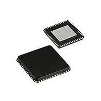
Manufacturer Part Number
CYRF69213-40LFXC
Description
IC PROC 8K FLASH 40VQFN
Manufacturer
Cypress Semiconductor Corp
Series
CYRFr
Type
Transceiverr
Datasheet
1.CYRF69213-40LFXC.pdf
(77 pages)
Specifications of CYRF69213-40LFXC
Package / Case
40-VQFN Exposed Pad, 40-HVQFN, 40-SQFN, 40-DHVQFN
Frequency
2.4GHz
Data Rate - Maximum
1Mbps
Modulation Or Protocol
ISM
Applications
General Purpose
Power - Output
4dBm
Sensitivity
-97dBm
Voltage - Supply
4 V ~ 5.5 V
Current - Receiving
23.4mA
Current - Transmitting
36.6mA
Data Interface
PCB, Surface Mount
Memory Size
8kB Flash, 256B SRAM
Antenna Connector
PCB, Surface Mount
Operating Temperature
0°C ~ 70°C
Operating Frequency
2497 MHz
Operating Supply Voltage
2.5 V or 3.3 V
Maximum Operating Temperature
+ 70 C
Minimum Operating Temperature
0 C
Mounting Style
SMD/SMT
Operating Temperature (min)
0C
Operating Temperature (max)
70C
Operating Temperature Classification
Commercial
Operating Supply Voltage (min)
1.8V
Operating Supply Voltage (typ)
2.5/3.3V
Operating Supply Voltage (max)
3.6V
Lead Free Status / RoHS Status
Lead free / RoHS Compliant
For Use With
770-1001 - ISP 4PORT CYPRESS ENCORE II MCU
Lead Free Status / Rohs Status
Lead free / RoHS Compliant
Other names
428-1934
Available stocks
Company
Part Number
Manufacturer
Quantity
Price

Part Number:
CYRF69213-40LFXC
Manufacturer:
CYPRESS/赛普拉斯
Quantity:
20 000


CPU Registers
Flags Register
The Flags Register can only be set or reset with logical
instruction.
Table 5. CPU Flags Register (CPU_F) [R/W]
Accumulator Register
Table 6. CPU Accumulator Register (CPU_A)
Document #: 001-07552 Rev. *D
Bits 7:5
Bit 4
Bit 3
Bit 2
Bit 1
Bit 0
Note CPU_F register is only readable with explicit register address 0xF7. The OR F, expr and AND F, expr instructions must be used
to set and clear the CPU_F bits
Bits 7:0
8-bit data value holds the result of any logical/arithmetic instruction that uses a source addressing mod
Read/Write –
Bit #
Field
Read/Write –
Default
Default
Field
Bit #
Reserved
XIO
Set by the user to select between the register banks
0 = Bank 0
1 = Bank 1
Super
Indicates whether the CPU is executing user code or Supervisor Code. (This code cannot be accessed directly by the
user.)
0 = User Code
1 = Supervisor Code
Carry
Set by CPU to indicate whether there has been a carry in the previous logical/arithmetic operation
0 = No Carry
1 = Carry
Zero
Set by CPU to indicate whether there has been a zero result in the previous logical/arithmetic operation
0 = Not Equal to Zero
1 = Equal to Zero
Global IE
Determines whether all interrupts are enabled or disabled
0 = Disabled
1 = Enabled
CPU Accumulator [7:0]
CPU Accumulator [7:0]
0
Reserved
0
7
7
–
0
–
0
6
6
–
0
–
0
5
5
XIO
R/W
0
–
0
4
4
Super
R
0
–
0
3
3
Carry
RW
0
–
0
2
2
Zero
RW
1
–
0
e
1
1
CYRF69213
Global IE
RW
0
–
0
Page 11 of 77
0
0
[+] Feedback
Related parts for CYRF69213-40LFXC
Image
Part Number
Description
Manufacturer
Datasheet
Request
R

Part Number:
Description:
Manufacturer:
Cypress Semiconductor Corp
Datasheet:
Part Number:
Description:
Manufacturer:
Cypress Semiconductor Corp
Datasheet:
Part Number:
Description:
Manufacturer:
Cypress Semiconductor Corp
Datasheet:
Part Number:
Description:
Manufacturer:
Cypress Semiconductor Corp
Datasheet:
Part Number:
Description:
Manufacturer:
Cypress Semiconductor Corp
Datasheet: