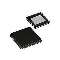
CYRF69213-40LFXC Cypress Semiconductor Corp, CYRF69213-40LFXC Datasheet - Page 42

CYRF69213-40LFXC
Manufacturer Part Number
CYRF69213-40LFXC
Description
IC PROC 8K FLASH 40VQFN
Manufacturer
Cypress Semiconductor Corp
Series
CYRFr
Type
Transceiverr
Datasheet
1.CYRF69213-40LFXC.pdf
(77 pages)
Specifications of CYRF69213-40LFXC
Package / Case
40-VQFN Exposed Pad, 40-HVQFN, 40-SQFN, 40-DHVQFN
Frequency
2.4GHz
Data Rate - Maximum
1Mbps
Modulation Or Protocol
ISM
Applications
General Purpose
Power - Output
4dBm
Sensitivity
-97dBm
Voltage - Supply
4 V ~ 5.5 V
Current - Receiving
23.4mA
Current - Transmitting
36.6mA
Data Interface
PCB, Surface Mount
Memory Size
8kB Flash, 256B SRAM
Antenna Connector
PCB, Surface Mount
Operating Temperature
0°C ~ 70°C
Operating Frequency
2497 MHz
Operating Supply Voltage
2.5 V or 3.3 V
Maximum Operating Temperature
+ 70 C
Minimum Operating Temperature
0 C
Mounting Style
SMD/SMT
Operating Temperature (min)
0C
Operating Temperature (max)
70C
Operating Temperature Classification
Commercial
Operating Supply Voltage (min)
1.8V
Operating Supply Voltage (typ)
2.5/3.3V
Operating Supply Voltage (max)
3.6V
Lead Free Status / RoHS Status
Lead free / RoHS Compliant
For Use With
770-1001 - ISP 4PORT CYPRESS ENCORE II MCU
Lead Free Status / Rohs Status
Lead free / RoHS Compliant
Other names
428-1934
Available stocks
Company
Part Number
Manufacturer
Quantity
Price
Part Number:
CYRF69213-40LFXC
Manufacturer:
CYPRESS/赛普拉斯
Quantity:
20 000
Table 58. P2 Configuration (P2CR) [0x15] [R/W]
GPIO Configurations for Low Power Mode:
To ensure low power mode, unbonded GPIO pins in CYRF69213 must be placed in a non floating state. The following assembly code
snippet shows how this is achieved. This snippet can be added as a part of the initialization routine.
//Code Snippet for addressing unbonded GPIOs
mov A, 00h
mov reg[1Fh],A
mov A, 01h
mov reg[16h],A // Port3 Configuration register - Enable ouptut
mov A, 00h
mov reg[03h],A // Asserting P3.0 and P3.1 outputs to '0'
mov A, 01h
mov reg[05h],A // Port0.0 Configuration register - Enable output
mov reg[07h],A // Port0.2 Configuration register - Enable output
mov reg[0Ah],A // Port0.5 Configuration register - Enable output
mov reg[0Bh],A // Port0.6 Configuration register - Enable output
mov A,reg[00h]
mov A,00h
and A,9Ah
mov reg[00h], A // Asserting outputs '0' to pins in port 1
When writing to port 0 , to access GPIOs P0.1,3,4,7 , mask bits 0,2,5,6 .Failing to do so will void the low power
Document #: 001-07552 Rev. *D
Bit #
Field
Read/Write
Default
This register only exists in CY7C638xx. This register controls the operation of pins P2.0–P2.1. In the CY7C638xx, only 8 mA sink drive capability is
available on this pin regardless of the setting of the High Sink bit
Reserved
7
–
0
Int Enable
R/W
6
0
Int Act Low
R/W
5
0
TTL Thresh
R/W
4
0
High Sink
R/W
3
0
Open Drain
R/W
2
0
Pull up Enable Output Enable
R/W
1
0
CYRF69213
Page 42 of 77
R/W
0
0
[+] Feedback


