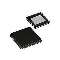
CYRF69213-40LFXC Cypress Semiconductor Corp, CYRF69213-40LFXC Datasheet - Page 22

CYRF69213-40LFXC
Manufacturer Part Number
CYRF69213-40LFXC
Description
IC PROC 8K FLASH 40VQFN
Manufacturer
Cypress Semiconductor Corp
Series
CYRFr
Type
Transceiverr
Datasheet
1.CYRF69213-40LFXC.pdf
(77 pages)
Specifications of CYRF69213-40LFXC
Package / Case
40-VQFN Exposed Pad, 40-HVQFN, 40-SQFN, 40-DHVQFN
Frequency
2.4GHz
Data Rate - Maximum
1Mbps
Modulation Or Protocol
ISM
Applications
General Purpose
Power - Output
4dBm
Sensitivity
-97dBm
Voltage - Supply
4 V ~ 5.5 V
Current - Receiving
23.4mA
Current - Transmitting
36.6mA
Data Interface
PCB, Surface Mount
Memory Size
8kB Flash, 256B SRAM
Antenna Connector
PCB, Surface Mount
Operating Temperature
0°C ~ 70°C
Operating Frequency
2497 MHz
Operating Supply Voltage
2.5 V or 3.3 V
Maximum Operating Temperature
+ 70 C
Minimum Operating Temperature
0 C
Mounting Style
SMD/SMT
Operating Temperature (min)
0C
Operating Temperature (max)
70C
Operating Temperature Classification
Commercial
Operating Supply Voltage (min)
1.8V
Operating Supply Voltage (typ)
2.5/3.3V
Operating Supply Voltage (max)
3.6V
Lead Free Status / RoHS Status
Lead free / RoHS Compliant
For Use With
770-1001 - ISP 4PORT CYPRESS ENCORE II MCU
Lead Free Status / Rohs Status
Lead free / RoHS Compliant
Other names
428-1934
Available stocks
Company
Part Number
Manufacturer
Quantity
Price
Part Number:
CYRF69213-40LFXC
Manufacturer:
CYPRESS/赛普拉斯
Quantity:
20 000
SROM Table Read Description
The Silicon IDs for enCoRe II devices are stored in SROM tables in the part, as shown in
The Silicon ID can be read out from the part using SROM Table reads. This is demonstrated in the following pseudo code. As
mentioned in the section
and their definition in given in the section
AREA SSCParmBlkA(RAM,ABS)
SSC_KEY1:
SSC_RETURNCODE:
SSC_KEY2 :
SSC_BLOCKID:
SSC_POINTER:
SSC_CLOCK:
SSC_MODE:
SSC_DELAY:
SSC_WRITE_ResultCode: blk 1 ; FFh
_main:
//Call SROM operation to read the SROM table
// At the end of the SSC command the silicon ID is stored in F8 (MSB) and F9(LSB) of the SRAM
.terminate:
Document #: 001-07552 Rev. *D
; load the supervisory code for flash operations
org
jmp .terminate
F8h // Variables are defined starting at address F8h
mov
mov
add
mov
mov
mov
SSC
mov
mov
X, SP
A, X
A, 3
[SSC_KEY2], A
[SSC_KEY1], 3Ah
A,6
A, 0
[SSC_BLOCKID], A// To read from Table 0 - Silicon ID is stored in Table 0
SROM
Table 0
Table 1
Table 2
Table 3
Table 4
Table 5
Table 6
Table 7
blk 1 ; F8h
blk 1
blk 1 ; FAh
blk 1 ; FBh
blk 1 ; FCh
blk 1 ; FDh
blk 1 ; FEh
on page 18, the SROM variables occupy address F8h through FFh in the SRAM. Each of the variables
; F8h
; load A with specific operation. 06h is the code for Table read
;F9h
; copy SP into X
; A temp stored in X
; SSC call the supervisory ROM
Silicon ID
[15-8]
F8h
SROM
supervisory key
result code
supervisory stack ptr key
block ID
pointer to data buffer
Clock
ClockW ClockE multiplier
flash macro sequence delay count
;FLASH_OPER_KEY - 3Ah
temporary result code
; create 3 byte stack frame (2 + pushed A)
; save stack frame for supervisory code
on page 18.
Silicon ID
[7-0]
F9h
Figure 8. SROM Table
F8h
F8h
F8h
F8h
Figure
F8h
8.
F8h
CYRF69213
Page 22 of 77
Table 23
[+] Feedback


