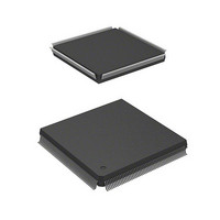
HD6417750RF200DV Renesas Electronics America, HD6417750RF200DV Datasheet - Page 871

HD6417750RF200DV
Manufacturer Part Number
HD6417750RF200DV
Description
MPU 1.5/3.3V 0K I-TEMP PB-FREE 2
Manufacturer
Renesas Electronics America
Series
SuperH® SH7750r
Datasheet
1.D6417750RBP240DV.pdf
(1164 pages)
Specifications of HD6417750RF200DV
Core Processor
SH-4
Core Size
32-Bit
Speed
200MHz
Connectivity
EBI/EMI, FIFO, SCI, SmartCard
Peripherals
DMA, POR, WDT
Number Of I /o
28
Program Memory Type
ROMless
Ram Size
48K x 8
Voltage - Supply (vcc/vdd)
1.35 V ~ 1.6 V
Oscillator Type
External
Operating Temperature
-40°C ~ 85°C
Package / Case
208-QFP Exposed Pad, 208-eQFP, 208-HQFP
Lead Free Status / RoHS Status
Lead free / RoHS Compliant
Eeprom Size
-
Program Memory Size
-
Data Converters
-
Available stocks
Company
Part Number
Manufacturer
Quantity
Price
Company:
Part Number:
HD6417750RF200DV
Manufacturer:
FREESCALE
Quantity:
450
- Current page: 871 of 1164
- Download datasheet (7Mb)
4. The receiving station carries out a parity check.
5. If the transmitting station does not receive an error signal, it proceeds to transmit the next data
17.3.4
Table 17.3 shows a bit map of the registers used by the smart card interface. Bits indicated as 0 or
1 must be set to the value shown. The setting of other bits is described below.
Table 17.3 Smart Card Interface Register Settings
Register
SCSMR1
SCBRR1
SCSCR1
SCTDR1
SCSSR1
SCRDR1
SCSCMR1 —
SCSPTR1
Note: A dash indicates an unused bit.
Serial Mode Register (SCSMR1) Settings: The GM bit is used to select the timing of TEND flag
setting, and, together with the CKE1 and CKE0 bits in the serial control register (SCSCR1), to
select the clock output state.
The O/E bit is cleared to 0 if the IC card is of the direct convention type, and set to 1 if of the
inverse convention type.
If there is no parity error and the data is received normally, the receiving station waits for
reception of the next data.
If a parity error occurs, however, the receiving station outputs an error signal (DE, low-level)
to request retransmission of the data. After outputting the error signal for the prescribed length
of time, the receiving station places the signal line in the high-impedance state again. The
signal line is pulled high again by a pull-up resistor.
frame.
If it receives an error signal, however, it returns to step 2 and retransmits the erroneous data.
Register Settings
Bit 7
GM
BRR7
TIE
TDR7
TDRE
RDR7
EIO
Bit 6
0
BRR6
RIE
TDR6
RDRF
RDR6
—
—
Bit 5
1
BRR5
TE
TDR5
ORER
—
—
RDR5
Bit 4
O/E
BRR4
RE
TDR4
FER/ERS PER
RDR4
—
—
Bit
Bit 3
1
BRR3
0
TDR3
RDR3
SDIR
SPB1IO
Rev.7.00 Oct. 10, 2008 Page 785 of 1074
Section 17 Smart Card Interface
Bit 2
0
BRR2
0
TDR2
TEND
RDR2
SINV
SPB1DT SPB0IO
Bit 1
CKS1
BRR1
CKE1
TDR1
0
RDR1
—
REJ09B0366-0700
Bit 0
CKS0
BRR0
CKE0
TDR0
0
RDR0
SMIF
SPB0DT
Related parts for HD6417750RF200DV
Image
Part Number
Description
Manufacturer
Datasheet
Request
R

Part Number:
Description:
KIT STARTER FOR M16C/29
Manufacturer:
Renesas Electronics America
Datasheet:

Part Number:
Description:
KIT STARTER FOR R8C/2D
Manufacturer:
Renesas Electronics America
Datasheet:

Part Number:
Description:
R0K33062P STARTER KIT
Manufacturer:
Renesas Electronics America
Datasheet:

Part Number:
Description:
KIT STARTER FOR R8C/23 E8A
Manufacturer:
Renesas Electronics America
Datasheet:

Part Number:
Description:
KIT STARTER FOR R8C/25
Manufacturer:
Renesas Electronics America
Datasheet:

Part Number:
Description:
KIT STARTER H8S2456 SHARPE DSPLY
Manufacturer:
Renesas Electronics America
Datasheet:

Part Number:
Description:
KIT STARTER FOR R8C38C
Manufacturer:
Renesas Electronics America
Datasheet:

Part Number:
Description:
KIT STARTER FOR R8C35C
Manufacturer:
Renesas Electronics America
Datasheet:

Part Number:
Description:
KIT STARTER FOR R8CL3AC+LCD APPS
Manufacturer:
Renesas Electronics America
Datasheet:

Part Number:
Description:
KIT STARTER FOR RX610
Manufacturer:
Renesas Electronics America
Datasheet:

Part Number:
Description:
KIT STARTER FOR R32C/118
Manufacturer:
Renesas Electronics America
Datasheet:

Part Number:
Description:
KIT DEV RSK-R8C/26-29
Manufacturer:
Renesas Electronics America
Datasheet:

Part Number:
Description:
KIT STARTER FOR SH7124
Manufacturer:
Renesas Electronics America
Datasheet:

Part Number:
Description:
KIT STARTER FOR H8SX/1622
Manufacturer:
Renesas Electronics America
Datasheet:

Part Number:
Description:
KIT DEV FOR SH7203
Manufacturer:
Renesas Electronics America
Datasheet:


