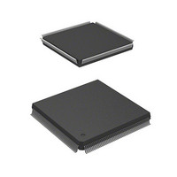
HD6417750RF200DV Renesas Electronics America, HD6417750RF200DV Datasheet - Page 217

HD6417750RF200DV
Manufacturer Part Number
HD6417750RF200DV
Description
MPU 1.5/3.3V 0K I-TEMP PB-FREE 2
Manufacturer
Renesas Electronics America
Series
SuperH® SH7750r
Datasheet
1.D6417750RBP240DV.pdf
(1164 pages)
Specifications of HD6417750RF200DV
Core Processor
SH-4
Core Size
32-Bit
Speed
200MHz
Connectivity
EBI/EMI, FIFO, SCI, SmartCard
Peripherals
DMA, POR, WDT
Number Of I /o
28
Program Memory Type
ROMless
Ram Size
48K x 8
Voltage - Supply (vcc/vdd)
1.35 V ~ 1.6 V
Oscillator Type
External
Operating Temperature
-40°C ~ 85°C
Package / Case
208-QFP Exposed Pad, 208-eQFP, 208-HQFP
Lead Free Status / RoHS Status
Lead free / RoHS Compliant
Eeprom Size
-
Program Memory Size
-
Data Converters
-
Available stocks
Company
Part Number
Manufacturer
Quantity
Price
Company:
Part Number:
HD6417750RF200DV
Manufacturer:
FREESCALE
Quantity:
450
- Current page: 217 of 1164
- Download datasheet (7Mb)
4.4.3
Setting CCR.IIX to 1 enables IC indexing to be performed using bit [25] of the effective address.
This is called IC index mode. In normal mode, with CCR.IIX cleared to 0, IC indexing is
performed using bits [12:5] of the effective address. Using index mode allows the IC to be handled
as two areas by means of effective address bit [25], providing efficient use of the cache.
4.5
To enable the IC and OC to be managed by software, their contents can be read and written by a
P2 area program with a MOV instruction in privileged mode. Operation is not guaranteed if access
is made from a program in another area. In this case, a branch to the P0, U0, P1, or P3 area should
be made at least 8 instructions after this MOV instruction. The IC and OC are allocated to the P4
area in physical memory space. Only data accesses can be used on both the IC address array and
data array and the OC address array and data array, and accesses are always longword-size.
Instruction fetches cannot be performed in these areas. For reserved bits, a write value of 0 should
be specified; their read value is undefined.
4.5.1
The IC address array is allocated to addresses H'F000 0000 to H'F0FF FFFF in the P4 area. An
address array access requires a 32-bit address field specification (when reading or writing) and a
32-bit data field specification. The entry to be accessed is specified in the address field, and the
write tag and V bit are specified in the data field.
In the address field, bits [31:24] have the value H'F0 indicating the IC address array, and the entry
is specified by bits [12:5]. CCR.IIX has no effect on this entry specification. The address array bit
[3] association bit (A bit) specifies whether or not association is performed when writing to the IC
address array. As only longword access is used, 0 should be specified for address field bits [1:0].
In the data field, the tag is indicated by bits [31:10], and the V bit by bit [0]. As the IC address
array tag is 19 bits in length, data field bits [31:29] are not used in the case of a write in which
association is not performed. Data field bits [31:29] are used for the virtual address specification
only in the case of a write in which association is performed.
The following three kinds of operation can be used on the IC address array:
IC Index Mode
Memory-Mapped Cache Configuration (SH7750, SH7750S)
IC Address Array
Rev.7.00 Oct. 10, 2008 Page 131 of 1074
REJ09B0366-0700
Section 4 Caches
Related parts for HD6417750RF200DV
Image
Part Number
Description
Manufacturer
Datasheet
Request
R

Part Number:
Description:
KIT STARTER FOR M16C/29
Manufacturer:
Renesas Electronics America
Datasheet:

Part Number:
Description:
KIT STARTER FOR R8C/2D
Manufacturer:
Renesas Electronics America
Datasheet:

Part Number:
Description:
R0K33062P STARTER KIT
Manufacturer:
Renesas Electronics America
Datasheet:

Part Number:
Description:
KIT STARTER FOR R8C/23 E8A
Manufacturer:
Renesas Electronics America
Datasheet:

Part Number:
Description:
KIT STARTER FOR R8C/25
Manufacturer:
Renesas Electronics America
Datasheet:

Part Number:
Description:
KIT STARTER H8S2456 SHARPE DSPLY
Manufacturer:
Renesas Electronics America
Datasheet:

Part Number:
Description:
KIT STARTER FOR R8C38C
Manufacturer:
Renesas Electronics America
Datasheet:

Part Number:
Description:
KIT STARTER FOR R8C35C
Manufacturer:
Renesas Electronics America
Datasheet:

Part Number:
Description:
KIT STARTER FOR R8CL3AC+LCD APPS
Manufacturer:
Renesas Electronics America
Datasheet:

Part Number:
Description:
KIT STARTER FOR RX610
Manufacturer:
Renesas Electronics America
Datasheet:

Part Number:
Description:
KIT STARTER FOR R32C/118
Manufacturer:
Renesas Electronics America
Datasheet:

Part Number:
Description:
KIT DEV RSK-R8C/26-29
Manufacturer:
Renesas Electronics America
Datasheet:

Part Number:
Description:
KIT STARTER FOR SH7124
Manufacturer:
Renesas Electronics America
Datasheet:

Part Number:
Description:
KIT STARTER FOR H8SX/1622
Manufacturer:
Renesas Electronics America
Datasheet:

Part Number:
Description:
KIT DEV FOR SH7203
Manufacturer:
Renesas Electronics America
Datasheet:


