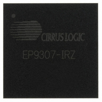
EP9307-IRZ Cirrus Logic Inc, EP9307-IRZ Datasheet - Page 659

EP9307-IRZ
Manufacturer Part Number
EP9307-IRZ
Description
IC ARM9 SOC ARM920T 272TFBGA
Manufacturer
Cirrus Logic Inc
Series
EP9r
Datasheets
1.EP9307-CRZ.pdf
(16 pages)
2.EP9307-CRZ.pdf
(50 pages)
3.EP9307-CRZ.pdf
(824 pages)
4.EP9307-CRZ.pdf
(48 pages)
Specifications of EP9307-IRZ
Core Size
16/32-Bit
Core Processor
ARM9
Speed
200MHz
Connectivity
EBI/EMI, Ethernet, I²C, IrDA, Keypad/Touchscreen, SPI, UART/USART, USB
Peripherals
AC'97, DMA, I²:S, LCD, LED, MaverickKey, POR, PWM, WDT
Number Of I /o
14
Program Memory Type
ROMless
Ram Size
32K x 8
Voltage - Supply (vcc/vdd)
1.65 V ~ 3.6 V
Data Converters
A/D 8x12b
Oscillator Type
External
Operating Temperature
-40°C ~ 85°C
Package / Case
272-TFBGA
Controller Family/series
(ARM9)
No. Of I/o's
14
Ram Memory Size
32MB
Cpu Speed
200MHz
No. Of Timers
3
No. Of Pwm Channels
1
Digital Ic Case Style
TFBGA
Embedded Interface Type
AC97, I2S, SPI, UART, USB
Rohs Compliant
Yes
Processor Series
EP93xx
Core
ARM920T
Data Bus Width
32 bit
3rd Party Development Tools
MDK-ARM, RL-ARM, ULINK2
Development Tools By Supplier
EDB9307A-Z
Lead Free Status / RoHS Status
Lead free / RoHS Compliant
For Use With
598-1133 - KIT DEVELOPMENT EP9307 ARM9
Eeprom Size
-
Program Memory Size
-
Lead Free Status / Rohs Status
Details
Other names
598-1256
Available stocks
Company
Part Number
Manufacturer
Quantity
Price
Company:
Part Number:
EP9307-IRZ
Manufacturer:
CIRRUS
Quantity:
3 468
Company:
Part Number:
EP9307-IRZR
Manufacturer:
Cirrus Logic Inc
Quantity:
10 000
- EP9307-CRZ PDF datasheet
- EP9307-CRZ PDF datasheet #2
- EP9307-CRZ PDF datasheet #3
- EP9307-CRZ PDF datasheet #4
- Current page: 659 of 824
- Download datasheet (13Mb)
DS785UM1
Each channel has a 16 deep by 32bit wide FIFO where the ARM or DMA controller can write
up to 8 sets of left/right data pairs before enabling the channel for transmission. In order to fill
the FIFO the following sequence of events must be performed by the programmer. (NOTE:
The following discussion is with respect to 1 channel only but applies to all.)
1. Enable I
2. Write to the FIFO: Once the I
• Supports 16/24/32 bit word lengths.
• Programmable left/right word clock polarity on the serial frame.
• Programmable Bit Clock polarity.
• Programmable data validity, that is, data valid on the rising/negative edge of the bit
• Programmable first data bit position (I
• Programmable Left or Right data word justification
• Programmable data shift direction, that is, MSB or LSB transmitted first.
• Data underflow detection, that is, re-transmission of old data.
• Clock domain synchronization.
• DMA access.
in order to turn on the PCLK to the I
correctly if this is not done.
clock.
either the DMA or the ARM.
can hold one left and one right stereo sample (16, 24 or 32 bits per sample). For APB
accesses, the left and right samples must be written to different addresses: I2STX0Lft
register address for left samples and I2STX0Rt register address for right samples (see
register definitions).
corresponding to left and right stereo data, to the FIFO. Only when both words are
written by the programmer will the FIFO be loaded. Assuming this is the first FIFO write,
Each FIFO is split up into 8 locations. Each location consists of 2 X 32bit register and
In order to fill a FIFO location, the programmer must write two data words,
7
1
0
:
:
2
S controller: The I
Right Sample 7
Left Sample 7
Right Sample 6
Right Sample 0
Left Sample 1
Right Sample 0
Left Sample 0
:
:
Copyright 2007 Cirrus Logic
2
S global control register bit, I2SGlCtrl[0] must be written to
2
Table 21-3. Transmitter FIFO’s
S controller is enabled, the TX FIFO may be written to by
Byte 7
Byte 3
Byte 7
Byte 7
Byte 3
Byte 7
Byte 3
:
:
2
S controller. The I
2
S or non-I
Byte 6
Byte 2
Byte 6
Byte 6
Byte 2
Byte 6
Byte 2
:
:
2
S format).
2
S controller will not function
Byte 5
Byte 1
Byte 5
Byte 5
Byte 1
Byte 5
Byte 1
:
:
EP93xx User’s Guide
Byte 4
Byte 0
Byte 4
Byte 4
Byte 0
Byte 4
Byte 0
:
:
I
2
S Controller
21-3
21
Related parts for EP9307-IRZ
Image
Part Number
Description
Manufacturer
Datasheet
Request
R

Part Number:
Description:
IC ARM9 SOC ARM920T 272TFBGA
Manufacturer:
Cirrus Logic Inc
Datasheet:

Part Number:
Description:
IC Universal Platform ARM9 SOC Prcessor
Manufacturer:
Cirrus Logic Inc
Datasheet:

Part Number:
Description:
IC Universal Platform ARM9 SOC Prcessor
Manufacturer:
Cirrus Logic Inc

Part Number:
Description:
IC,MICROPROCESSOR,32-BIT,CMOS,BGA,272PIN,PLASTIC
Manufacturer:
Cirrus Logic Inc
Datasheet:

Part Number:
Description:
IC Universal Platform ARM9 SOC Prcessor
Manufacturer:
Cirrus Logic Inc
Datasheet:

Part Number:
Description:
Microcontrollers (MCU) IC Universal Platfrm ARM9 SOC Prcessor
Manufacturer:
Cirrus Logic Inc

Part Number:
Description:
Microcontrollers (MCU) IC Universal Platfrm ARM9 SOC Prcessor
Manufacturer:
Cirrus Logic Inc

Part Number:
Description:
MCU, MPU & DSP Development Tools Eval Bd Uni. ARM9 SOC Processor
Manufacturer:
Cirrus Logic Inc
Datasheet:

Part Number:
Description:
Development Kit
Manufacturer:
Cirrus Logic Inc
Datasheet:

Part Number:
Description:
Development Kit
Manufacturer:
Cirrus Logic Inc
Datasheet:

Part Number:
Description:
High-efficiency PFC + Fluorescent Lamp Driver Reference Design
Manufacturer:
Cirrus Logic Inc
Datasheet:

Part Number:
Description:
Development Kit
Manufacturer:
Cirrus Logic Inc
Datasheet:

Part Number:
Description:
Ref Bd For Speakerbar MSA & DSP Products
Manufacturer:
Cirrus Logic Inc


