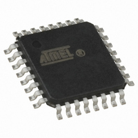
ATMEGA168-15AZ Atmel, ATMEGA168-15AZ Datasheet - Page 81

ATMEGA168-15AZ
Manufacturer Part Number
ATMEGA168-15AZ
Description
MCU AVR 16K FLASH 15MHZ 32-TQFP
Manufacturer
Atmel
Series
AVR® ATmegar
Datasheet
1.ATMEGA168-15AZ.pdf
(340 pages)
Specifications of ATMEGA168-15AZ
Package / Case
32-TQFP, 32-VQFP
Voltage - Supply (vcc/vdd)
2.7 V ~ 5.5 V
Operating Temperature
-40°C ~ 125°C
Speed
16MHz
Number Of I /o
23
Eeprom Size
512 x 8
Core Processor
AVR
Program Memory Type
FLASH
Ram Size
1K x 8
Program Memory Size
16KB (16K x 8)
Data Converters
A/D 8x10b
Oscillator Type
Internal
Peripherals
Brown-out Detect/Reset, POR, PWM, WDT
Connectivity
I²C, SPI, UART/USART
Core Size
8-Bit
Cpu Family
ATmega
Device Core
AVR
Device Core Size
8b
Frequency (max)
16MHz
Interface Type
2-Wire/USART/Serial
Total Internal Ram Size
1KB
# I/os (max)
23
Number Of Timers - General Purpose
3
Operating Supply Voltage (typ)
3.3/5V
Operating Supply Voltage (max)
5.5V
Operating Supply Voltage (min)
2.7V
On-chip Adc
8-chx10-bit
Instruction Set Architecture
RISC
Operating Temp Range
-40C to 125C
Operating Temperature Classification
Automotive
Mounting
Surface Mount
Pin Count
32
Package Type
TQFP
Lead Free Status / RoHS Status
Lead free / RoHS Compliant
Available stocks
Company
Part Number
Manufacturer
Quantity
Price
- Current page: 81 of 340
- Download datasheet (6Mb)
10.4.9
11. External Interrupts
11.0.1
7530I–AVR–02/10
The Port D Input Pins Address – PIND
External Interrupt Control Register A – EICRA
The External Interrupts are triggered by the INT0 and INT1 pins or any of the PCINT23..0 pins.
Observe that, if enabled, the interrupts will trigger even if the INT0 and INT1 or PCINT23..0 pins
are configured as outputs. This feature provides a way of generating a software interrupt. The
pin change interrupt PCI2 will trigger if any enabled PCINT23..16 pin toggles. The pin change
interrupt PCI1 will trigger if any enabled PCINT14..8 pin toggles. The pin change interrupt PCI0
will trigger if any enabled PCINT7..0 pin toggles. The PCMSK2, PCMSK1 and PCMSK0 Regis-
ters control which pins contribute to the pin change interrupts. Pin change interrupts on
PCINT23..0 are detected asynchronously. This implies that these interrupts can be used for
waking the part also from sleep modes other than Idle mode.
The INT0 and INT1 interrupts can be triggered by a falling or rising edge or a low level. This is
set up as indicated in the specification for the External Interrupt Control Register A – EICRA.
When the INT0 or INT1 interrupts are enabled and are configured as level triggered, the inter-
rupts will trigger as long as the pin is held low. Note that recognition of falling or rising edge
interrupts on INT0 or INT1 requires the presence of an I/O clock, described in
and their Distribution” on page
nously. This implies that this interrupt can be used for waking the part also from sleep modes
other than Idle mode. The I/O clock is halted in all sleep modes except Idle mode.
Note that if a level triggered interrupt is used for wake-up from Power-down, the required level
must be held long enough for the MCU to complete the wake-up to trigger the level interrupt. If
the level disappears before the end of the Start-up Time, the MCU will still wake up, but no inter-
rupt will be generated. The start-up time is defined by the SUT and CKSEL Fuses as described
in
The External Interrupt Control Register A contains control bits for interrupt sense control.
• Bit 7..4 – Res: Reserved Bits
These bits are unused bits in the ATmega48/88/168, and will always read as zero.
• Bit 3, 2 – ISC11, ISC10: Interrupt Sense Control 1 Bit 1 and Bit 0
The External Interrupt 1 is activated by the external pin INT1 if the SREG I-flag and the corre-
sponding interrupt mask are set. The level and edges on the external INT1 pin that activate the
interrupt are defined in
edges. If edge or toggle interrupt is selected, pulses that last longer than one clock period will
generate an interrupt. Shorter pulses are not guaranteed to generate an interrupt. If low level
interrupt is selected, the low level must be held until the completion of the currently executing
instruction to generate an interrupt.
Bit
Read/Write
Initial Value
Bit
Read/Write
Initial Value
“System Clock and Clock Options” on page
PIND7
N/A
R
7
R
7
–
0
PIND6
N/A
Table
R
6
R
6
–
0
24. Low level interrupt on INT0 and INT1 is detected asynchro-
11-1. The value on the INT1 pin is sampled before detecting
PIND5
N/A
R
5
R
5
–
0
ATmega48/88/168 Automotive
PIND4
N/A
R
4
R
4
–
0
24.
PIND3
ISC11
R/W
N/A
R
3
3
0
ISC10
PIND2
R/W
N/A
2
0
R
2
ISC01
PIND1
R/W
N/A
1
0
R
1
ISC00
PIND0
R/W
“Clock Systems
N/A
0
0
R
0
EICRA
PIND
81
Related parts for ATMEGA168-15AZ
Image
Part Number
Description
Manufacturer
Datasheet
Request
R

Part Number:
Description:
Manufacturer:
Atmel Corporation
Datasheet:

Part Number:
Description:
Manufacturer:
Atmel Corporation
Datasheet:

Part Number:
Description:
Manufacturer:
ATMEL Corporation
Datasheet:

Part Number:
Description:
IC AVR MCU 16K 20MHZ 32TQFP
Manufacturer:
Atmel
Datasheet:

Part Number:
Description:
IC AVR MCU 16K 20MHZ 32-QFN
Manufacturer:
Atmel
Datasheet:

Part Number:
Description:
IC AVR MCU 16K 20MHZ 28DIP
Manufacturer:
Atmel
Datasheet:

Part Number:
Description:
MCU AVR 16K FLASH 15MHZ 32-QFN
Manufacturer:
Atmel
Datasheet:

Part Number:
Description:
IC AVR MCU 16K 20MHZ 32TQFP
Manufacturer:
Atmel
Datasheet:

Part Number:
Description:
MCU AVR 16KB FLASH 20MHZ 32QFN
Manufacturer:
Atmel
Datasheet:

Part Number:
Description:
MCU AVR 16KB FLASH 20MHZ 32TQFP
Manufacturer:
Atmel
Datasheet:

Part Number:
Description:
IC MCU AVR 16K FLASH 32-QFN
Manufacturer:
Atmel
Datasheet:


