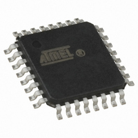
ATMEGA168-15AZ Atmel, ATMEGA168-15AZ Datasheet - Page 259

ATMEGA168-15AZ
Manufacturer Part Number
ATMEGA168-15AZ
Description
MCU AVR 16K FLASH 15MHZ 32-TQFP
Manufacturer
Atmel
Series
AVR® ATmegar
Datasheet
1.ATMEGA168-15AZ.pdf
(340 pages)
Specifications of ATMEGA168-15AZ
Package / Case
32-TQFP, 32-VQFP
Voltage - Supply (vcc/vdd)
2.7 V ~ 5.5 V
Operating Temperature
-40°C ~ 125°C
Speed
16MHz
Number Of I /o
23
Eeprom Size
512 x 8
Core Processor
AVR
Program Memory Type
FLASH
Ram Size
1K x 8
Program Memory Size
16KB (16K x 8)
Data Converters
A/D 8x10b
Oscillator Type
Internal
Peripherals
Brown-out Detect/Reset, POR, PWM, WDT
Connectivity
I²C, SPI, UART/USART
Core Size
8-Bit
Cpu Family
ATmega
Device Core
AVR
Device Core Size
8b
Frequency (max)
16MHz
Interface Type
2-Wire/USART/Serial
Total Internal Ram Size
1KB
# I/os (max)
23
Number Of Timers - General Purpose
3
Operating Supply Voltage (typ)
3.3/5V
Operating Supply Voltage (max)
5.5V
Operating Supply Voltage (min)
2.7V
On-chip Adc
8-chx10-bit
Instruction Set Architecture
RISC
Operating Temp Range
-40C to 125C
Operating Temperature Classification
Automotive
Mounting
Surface Mount
Pin Count
32
Package Type
TQFP
Lead Free Status / RoHS Status
Lead free / RoHS Compliant
Available stocks
Company
Part Number
Manufacturer
Quantity
Price
- Current page: 259 of 340
- Download datasheet (6Mb)
23.1.2
23.1.3
7530I–AVR–02/10
EEPROM Write Prevents Writing to SPMCSR
Reading the Fuse and Lock Bits from Software
• Bit 0 – SELFPRGEN: Self Programming Enable
This bit enables the SPM instruction for the next four clock cycles. If written to one together with
either RWWSRE, BLBSET, PGWRT, or PGERS, the following SPM instruction will have a spe-
cial meaning, see description above. If only SELFPRGEN is written, the following SPM
instruction will store the value in R1:R0 in the temporary page buffer addressed by the Z-pointer.
The LSB of the Z-pointer is ignored. The SELFPRGEN bit will auto-clear upon completion of an
SPM instruction, or if no SPM instruction is executed within four clock cycles. During Page Erase
and Page Write, the SELFPRGEN bit remains high until the operation is completed.
Writing any other combination than “10001”, “01001”, “00101”, “00011” or “00001” in the lower
five bits will have no effect.
Note that an EEPROM write operation will block all software programming to Flash. Reading the
Fuses and Lock bits from software will also be prevented during the EEPROM write operation. It
is recommended that the user checks the status bit (EEPE) in the EECR Register and verifies
that the bit is cleared before writing to the SPMCSR Register.
It is possible to read both the Fuse and Lock bits from software. To read the Lock bits, load the
Z-pointer with 0x0001 and set the BLBSET and SELFPRGEN bits in SPMCSR. When an LPM
instruction is executed within three CPU cycles after the BLBSET and SELFPRGEN bits are set
in SPMCSR, the value of the Lock bits will be loaded in the destination register. The BLBSET
and SELFPRGEN bits will auto-clear upon completion of reading the Lock bits or if no LPM
instruction is executed within three CPU cycles or no SPM instruction is executed within four
CPU cycles. When BLBSET and SELFPRGEN are cleared, LPM will work as described in the
Instruction set Manual.
The algorithm for reading the Fuse Low byte is similar to the one described above for reading
the Lock bits. To read the Fuse Low byte, load the Z-pointer with 0x0000 and set the BLBSET
and SELFPRGEN bits in SPMCSR. When an LPM instruction is executed within three cycles
after the BLBSET and SELFPRGEN bits are set in the SPMCSR, the value of the Fuse Low byte
(FLB) will be loaded in the destination register as shown below.See
a detailed description and mapping of the Fuse Low byte.
Similarly, when reading the Fuse High byte (FHB), load 0x0003 in the Z-pointer. When an LPM
instruction is executed within three cycles after the BLBSET and SELFPRGEN bits are set in the
SPMCSR, the value of the Fuse High byte will be loaded in the destination register as shown
below. See
byte.
Bit
Rd
Bit
Rd
Bit
Rd
Table 25-4 on page 280
FHB7
FLB7
7
7
7
–
FHB6
FLB6
6
6
6
–
FLB5
FHB5
5
–
5
5
for detailed description and mapping of the Extended Fuse
ATmega48/88/168 Automotive
FLB4
FHB4
4
–
4
4
FLB3
FHB3
3
–
3
3
FHB2
FLB2
2
–
2
2
Table 25-5 on page 280
FHB1
FLB1
LB2
1
1
1
FHB0
FLB0
LB1
0
0
0
259
for
Related parts for ATMEGA168-15AZ
Image
Part Number
Description
Manufacturer
Datasheet
Request
R

Part Number:
Description:
Manufacturer:
Atmel Corporation
Datasheet:

Part Number:
Description:
Manufacturer:
Atmel Corporation
Datasheet:

Part Number:
Description:
Manufacturer:
ATMEL Corporation
Datasheet:

Part Number:
Description:
IC AVR MCU 16K 20MHZ 32TQFP
Manufacturer:
Atmel
Datasheet:

Part Number:
Description:
IC AVR MCU 16K 20MHZ 32-QFN
Manufacturer:
Atmel
Datasheet:

Part Number:
Description:
IC AVR MCU 16K 20MHZ 28DIP
Manufacturer:
Atmel
Datasheet:

Part Number:
Description:
MCU AVR 16K FLASH 15MHZ 32-QFN
Manufacturer:
Atmel
Datasheet:

Part Number:
Description:
IC AVR MCU 16K 20MHZ 32TQFP
Manufacturer:
Atmel
Datasheet:

Part Number:
Description:
MCU AVR 16KB FLASH 20MHZ 32QFN
Manufacturer:
Atmel
Datasheet:

Part Number:
Description:
MCU AVR 16KB FLASH 20MHZ 32TQFP
Manufacturer:
Atmel
Datasheet:

Part Number:
Description:
IC MCU AVR 16K FLASH 32-QFN
Manufacturer:
Atmel
Datasheet:


