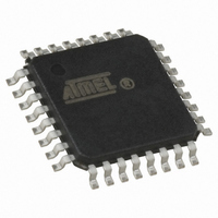
ATMEGA168-15AZ Atmel, ATMEGA168-15AZ Datasheet - Page 288

ATMEGA168-15AZ
Manufacturer Part Number
ATMEGA168-15AZ
Description
MCU AVR 16K FLASH 15MHZ 32-TQFP
Manufacturer
Atmel
Series
AVR® ATmegar
Datasheet
1.ATMEGA168-15AZ.pdf
(340 pages)
Specifications of ATMEGA168-15AZ
Package / Case
32-TQFP, 32-VQFP
Voltage - Supply (vcc/vdd)
2.7 V ~ 5.5 V
Operating Temperature
-40°C ~ 125°C
Speed
16MHz
Number Of I /o
23
Eeprom Size
512 x 8
Core Processor
AVR
Program Memory Type
FLASH
Ram Size
1K x 8
Program Memory Size
16KB (16K x 8)
Data Converters
A/D 8x10b
Oscillator Type
Internal
Peripherals
Brown-out Detect/Reset, POR, PWM, WDT
Connectivity
I²C, SPI, UART/USART
Core Size
8-Bit
Cpu Family
ATmega
Device Core
AVR
Device Core Size
8b
Frequency (max)
16MHz
Interface Type
2-Wire/USART/Serial
Total Internal Ram Size
1KB
# I/os (max)
23
Number Of Timers - General Purpose
3
Operating Supply Voltage (typ)
3.3/5V
Operating Supply Voltage (max)
5.5V
Operating Supply Voltage (min)
2.7V
On-chip Adc
8-chx10-bit
Instruction Set Architecture
RISC
Operating Temp Range
-40C to 125C
Operating Temperature Classification
Automotive
Mounting
Surface Mount
Pin Count
32
Package Type
TQFP
Lead Free Status / RoHS Status
Lead free / RoHS Compliant
Available stocks
Company
Part Number
Manufacturer
Quantity
Price
- Current page: 288 of 340
- Download datasheet (6Mb)
25.7.5
25.7.6
288
ATmega48/88/168 Automotive
Programming the EEPROM
Reading the Flash
The EEPROM is organized in pages, see
EEPROM, the program data is latched into a page buffer. This allows one page of data to be
programmed simultaneously. The programming algorithm for the EEPROM data memory is as
follows (refer to
Data loading):
K: Repeat 3 through 5 until the entire buffer is filled.
L: Program EEPROM page
Figure 25-4. Programming the EEPROM Waveforms
The algorithm for reading the Flash memory is as follows (refer to
page 286
1. A: Load Command “0001 0001”.
2. G: Load Address High Byte (0x00 - 0xFF).
3. B: Load Address Low Byte (0x00 - 0xFF).
4. C: Load Data (0x00 - 0xFF).
5. E: Latch data (give PAGEL a positive pulse).
1. Set BS1 to “0”.
2. Give WR a negative pulse. This starts programming of the EEPROM page. RDY/BSY
3. Wait until to RDY/BSY goes high before programming the next page (See
1. A: Load Command “0000 0010”.
2. G: Load Address High Byte (0x00 - 0xFF).
3. B: Load Address Low Byte (0x00 - 0xFF).
4. Set OE to “0”, and BS1 to “0”. The Flash word low byte can now be read at DATA.
5. Set BS1 to “1”. The Flash word high byte can now be read at DATA.
6. Set OE to “1”.
RESET +12V
goes low.
for signal waveforms).
RDY/BSY
PAGEL
XTAL1
DATA
XA1
XA0
BS1
BS2
WR
OE
for details on Command and Address loading):
“Programming the Flash” on page 286
0x11
A
ADDR. HIGH
G
ADDR. LOW
B
DATA
C
Table 25-13 on page
XX
E
ADDR. LOW
B
for details on Command, Address and
DATA
C
K
XX
E
284. When programming the
“Programming the Flash” on
L
Figure 25-4
7530I–AVR–02/10
Related parts for ATMEGA168-15AZ
Image
Part Number
Description
Manufacturer
Datasheet
Request
R

Part Number:
Description:
Manufacturer:
Atmel Corporation
Datasheet:

Part Number:
Description:
Manufacturer:
Atmel Corporation
Datasheet:

Part Number:
Description:
Manufacturer:
ATMEL Corporation
Datasheet:

Part Number:
Description:
IC AVR MCU 16K 20MHZ 32TQFP
Manufacturer:
Atmel
Datasheet:

Part Number:
Description:
IC AVR MCU 16K 20MHZ 32-QFN
Manufacturer:
Atmel
Datasheet:

Part Number:
Description:
IC AVR MCU 16K 20MHZ 28DIP
Manufacturer:
Atmel
Datasheet:

Part Number:
Description:
MCU AVR 16K FLASH 15MHZ 32-QFN
Manufacturer:
Atmel
Datasheet:

Part Number:
Description:
IC AVR MCU 16K 20MHZ 32TQFP
Manufacturer:
Atmel
Datasheet:

Part Number:
Description:
MCU AVR 16KB FLASH 20MHZ 32QFN
Manufacturer:
Atmel
Datasheet:

Part Number:
Description:
MCU AVR 16KB FLASH 20MHZ 32TQFP
Manufacturer:
Atmel
Datasheet:

Part Number:
Description:
IC MCU AVR 16K FLASH 32-QFN
Manufacturer:
Atmel
Datasheet:


