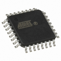
ATMEGA168-15AZ Atmel, ATMEGA168-15AZ Datasheet - Page 41

ATMEGA168-15AZ
Manufacturer Part Number
ATMEGA168-15AZ
Description
MCU AVR 16K FLASH 15MHZ 32-TQFP
Manufacturer
Atmel
Series
AVR® ATmegar
Datasheet
1.ATMEGA168-15AZ.pdf
(340 pages)
Specifications of ATMEGA168-15AZ
Package / Case
32-TQFP, 32-VQFP
Voltage - Supply (vcc/vdd)
2.7 V ~ 5.5 V
Operating Temperature
-40°C ~ 125°C
Speed
16MHz
Number Of I /o
23
Eeprom Size
512 x 8
Core Processor
AVR
Program Memory Type
FLASH
Ram Size
1K x 8
Program Memory Size
16KB (16K x 8)
Data Converters
A/D 8x10b
Oscillator Type
Internal
Peripherals
Brown-out Detect/Reset, POR, PWM, WDT
Connectivity
I²C, SPI, UART/USART
Core Size
8-Bit
Cpu Family
ATmega
Device Core
AVR
Device Core Size
8b
Frequency (max)
16MHz
Interface Type
2-Wire/USART/Serial
Total Internal Ram Size
1KB
# I/os (max)
23
Number Of Timers - General Purpose
3
Operating Supply Voltage (typ)
3.3/5V
Operating Supply Voltage (max)
5.5V
Operating Supply Voltage (min)
2.7V
On-chip Adc
8-chx10-bit
Instruction Set Architecture
RISC
Operating Temp Range
-40C to 125C
Operating Temperature Classification
Automotive
Mounting
Surface Mount
Pin Count
32
Package Type
TQFP
Lead Free Status / RoHS Status
Lead free / RoHS Compliant
Available stocks
Company
Part Number
Manufacturer
Quantity
Price
- Current page: 41 of 340
- Download datasheet (6Mb)
7.7.6
7.7.7
8. System Control and Reset
8.0.1
7530I–AVR–02/10
Port Pins
On-chip Debug System
Resetting the AVR
When entering a sleep mode, all port pins should be configured to use minimum power. The
most important is then to ensure that no pins drive resistive loads. In sleep modes where both
the I/O clock (clk
be disabled. This ensures that no power is consumed by the input logic when not needed. In
some cases, the input logic is needed for detecting wake-up conditions, and it will then be
enabled. Refer to the section
which pins are enabled. If the input buffer is enabled and the input signal is left floating or have
an analog signal level close to V
For analog input pins, the digital input buffer should be disabled at all times. An analog signal
level close to V
input buffers can be disabled by writing to the Digital Input Disable Registers (DIDR1 and
DIDR0). Refer to
able Register 0 – DIDR0” on page 253
If the On-chip debug system is enabled by the DWEN Fuse and the chip enters sleep mode, the
main clock source is enabled and hence always consumes power. In the deeper sleep modes,
this will contribute significantly to the total current consumption.
During reset, all I/O Registers are set to their initial values, and the program starts execution
from the Reset Vector. For the ATmega168, the instruction placed at the Reset Vector must be a
JMP – Absolute Jump – instruction to the reset handling routine. For the ATmega48 and
ATmega88, the instruction placed at the Reset Vector must be an RJMP – Relative Jump –
instruction to the reset handling routine. If the program never enables an interrupt source, the
Interrupt Vectors are not used, and regular program code can be placed at these locations. This
is also the case if the Reset Vector is in the Application section while the Interrupt Vectors are in
the Boot section or vice versa (ATmega88/168 only). The circuit diagram in
reset logic.
The I/O ports of the AVR are immediately reset to their initial state when a reset source goes
active. This does not require any clock source to be running.
After all reset sources have gone inactive, a delay counter is invoked, stretching the internal
reset. This allows the power to reach a stable level before normal operation starts. The time-out
period of the delay counter is defined by the user through the SUT and CKSEL Fuses. The dif-
ferent selections for the delay period are presented in
Table 8-1 on page 43
CC
I/O
“Digital Input Disable Register 1 – DIDR1” on page 236
/2 on an input pin can cause significant current even in active mode. Digital
) and the ADC clock (clk
“Digital Input Enable and Sleep Modes” on page 67
CC
defines the electrical parameters of the reset circuitry.
/2, the input buffer will use excessive power.
ATmega48/88/168 Automotive
for details.
ADC
) are stopped, the input buffers of the device will
“Clock Sources” on page
and
Figure 8-1
“Digital Input Dis-
25.
for details on
shows the
41
Related parts for ATMEGA168-15AZ
Image
Part Number
Description
Manufacturer
Datasheet
Request
R

Part Number:
Description:
Manufacturer:
Atmel Corporation
Datasheet:

Part Number:
Description:
Manufacturer:
Atmel Corporation
Datasheet:

Part Number:
Description:
Manufacturer:
ATMEL Corporation
Datasheet:

Part Number:
Description:
IC AVR MCU 16K 20MHZ 32TQFP
Manufacturer:
Atmel
Datasheet:

Part Number:
Description:
IC AVR MCU 16K 20MHZ 32-QFN
Manufacturer:
Atmel
Datasheet:

Part Number:
Description:
IC AVR MCU 16K 20MHZ 28DIP
Manufacturer:
Atmel
Datasheet:

Part Number:
Description:
MCU AVR 16K FLASH 15MHZ 32-QFN
Manufacturer:
Atmel
Datasheet:

Part Number:
Description:
IC AVR MCU 16K 20MHZ 32TQFP
Manufacturer:
Atmel
Datasheet:

Part Number:
Description:
MCU AVR 16KB FLASH 20MHZ 32QFN
Manufacturer:
Atmel
Datasheet:

Part Number:
Description:
MCU AVR 16KB FLASH 20MHZ 32TQFP
Manufacturer:
Atmel
Datasheet:

Part Number:
Description:
IC MCU AVR 16K FLASH 32-QFN
Manufacturer:
Atmel
Datasheet:


