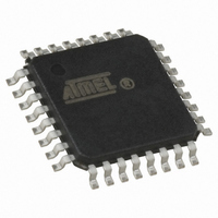
ATMEGA168-15AZ Atmel, ATMEGA168-15AZ Datasheet - Page 23

ATMEGA168-15AZ
Manufacturer Part Number
ATMEGA168-15AZ
Description
MCU AVR 16K FLASH 15MHZ 32-TQFP
Manufacturer
Atmel
Series
AVR® ATmegar
Datasheet
1.ATMEGA168-15AZ.pdf
(340 pages)
Specifications of ATMEGA168-15AZ
Package / Case
32-TQFP, 32-VQFP
Voltage - Supply (vcc/vdd)
2.7 V ~ 5.5 V
Operating Temperature
-40°C ~ 125°C
Speed
16MHz
Number Of I /o
23
Eeprom Size
512 x 8
Core Processor
AVR
Program Memory Type
FLASH
Ram Size
1K x 8
Program Memory Size
16KB (16K x 8)
Data Converters
A/D 8x10b
Oscillator Type
Internal
Peripherals
Brown-out Detect/Reset, POR, PWM, WDT
Connectivity
I²C, SPI, UART/USART
Core Size
8-Bit
Cpu Family
ATmega
Device Core
AVR
Device Core Size
8b
Frequency (max)
16MHz
Interface Type
2-Wire/USART/Serial
Total Internal Ram Size
1KB
# I/os (max)
23
Number Of Timers - General Purpose
3
Operating Supply Voltage (typ)
3.3/5V
Operating Supply Voltage (max)
5.5V
Operating Supply Voltage (min)
2.7V
On-chip Adc
8-chx10-bit
Instruction Set Architecture
RISC
Operating Temp Range
-40C to 125C
Operating Temperature Classification
Automotive
Mounting
Surface Mount
Pin Count
32
Package Type
TQFP
Lead Free Status / RoHS Status
Lead free / RoHS Compliant
Available stocks
Company
Part Number
Manufacturer
Quantity
Price
- Current page: 23 of 340
- Download datasheet (6Mb)
5.4
5.4.1
5.4.2
5.4.3
5.4.4
7530I–AVR–02/10
I/O Memory
General Purpose I/O Registers
General Purpose I/O Register 2 – GPIOR2
General Purpose I/O Register 1 – GPIOR1
General Purpose I/O Register 0 – GPIOR0
The I/O space definition of the ATmega48/88/168 is shown in
All ATmega48/88/168 I/Os and peripherals are placed in the I/O space. All I/O locations may be
accessed by the LD/LDS/LDD and ST/STS/STD instructions, transferring data between the 32
general purpose working registers and the I/O space. I/O Registers within the address range
0x00 - 0x1F are directly bit-accessible using the SBI and CBI instructions. In these registers, the
value of single bits can be checked by using the SBIS and SBIC instructions. Refer to the
instruction set section for more details. When using the I/O specific commands IN and OUT, the
I/O addresses 0x00 - 0x3F must be used. When addressing I/O Registers as data space using
LD and ST instructions, 0x20 must be added to these addresses. The ATmega48/88/168 is a
complex microcontroller with more peripheral units than can be supported within the 64 location
reserved in Opcode for the IN and OUT instructions. For the Extended I/O space from 0x60 -
0xFF in SRAM, only the ST/STS/STD and LD/LDS/LDD instructions can be used.
For compatibility with future devices, reserved bits should be written to zero if accessed.
Reserved I/O memory addresses should never be written.
Some of the Status Flags are cleared by writing a logical one to them. Note that, unlike most
other AVRs, the CBI and SBI instructions will only operate on the specified bit, and can therefore
be used on registers containing such Status Flags. The CBI and SBI instructions work with reg-
isters 0x00 to 0x1F only.
The I/O and peripherals control registers are explained in later sections.
The ATmega48/88/168 contains three General Purpose I/O Registers. These registers can be
used for storing any information, and they are particularly useful for storing global variables and
Status Flags. General Purpose I/O Registers within the address range 0x00 - 0x1F are directly
bit-accessible using the SBI, CBI, SBIS, and SBIC instructions.
Bit
Read/Write
Initial Value
Bit
Read/Write
Initial Value
Bit
Read/Write
Initial Value
MSB
MSB
MSB
R/W
R/W
R/W
7
0
7
0
7
0
R/W
R/W
R/W
6
0
6
0
6
0
R/W
R/W
R/W
5
0
5
0
5
0
ATmega48/88/168 Automotive
R/W
R/W
R/W
4
0
4
0
4
0
R/W
R/W
R/W
3
0
3
0
3
0
R/W
R/W
R/W
“Register Summary” on page
2
0
2
0
2
0
R/W
R/W
R/W
1
0
1
0
1
0
LSB
R/W
LSB
R/W
LSB
R/W
0
0
0
0
0
0
GPIOR2
GPIOR1
GPIOR0
318.
23
Related parts for ATMEGA168-15AZ
Image
Part Number
Description
Manufacturer
Datasheet
Request
R

Part Number:
Description:
Manufacturer:
Atmel Corporation
Datasheet:

Part Number:
Description:
Manufacturer:
Atmel Corporation
Datasheet:

Part Number:
Description:
Manufacturer:
ATMEL Corporation
Datasheet:

Part Number:
Description:
IC AVR MCU 16K 20MHZ 32TQFP
Manufacturer:
Atmel
Datasheet:

Part Number:
Description:
IC AVR MCU 16K 20MHZ 32-QFN
Manufacturer:
Atmel
Datasheet:

Part Number:
Description:
IC AVR MCU 16K 20MHZ 28DIP
Manufacturer:
Atmel
Datasheet:

Part Number:
Description:
MCU AVR 16K FLASH 15MHZ 32-QFN
Manufacturer:
Atmel
Datasheet:

Part Number:
Description:
IC AVR MCU 16K 20MHZ 32TQFP
Manufacturer:
Atmel
Datasheet:

Part Number:
Description:
MCU AVR 16KB FLASH 20MHZ 32QFN
Manufacturer:
Atmel
Datasheet:

Part Number:
Description:
MCU AVR 16KB FLASH 20MHZ 32TQFP
Manufacturer:
Atmel
Datasheet:

Part Number:
Description:
IC MCU AVR 16K FLASH 32-QFN
Manufacturer:
Atmel
Datasheet:


