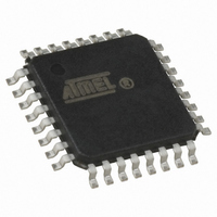
ATMEGA168-15AZ Atmel, ATMEGA168-15AZ Datasheet - Page 181

ATMEGA168-15AZ
Manufacturer Part Number
ATMEGA168-15AZ
Description
MCU AVR 16K FLASH 15MHZ 32-TQFP
Manufacturer
Atmel
Series
AVR® ATmegar
Datasheet
1.ATMEGA168-15AZ.pdf
(340 pages)
Specifications of ATMEGA168-15AZ
Package / Case
32-TQFP, 32-VQFP
Voltage - Supply (vcc/vdd)
2.7 V ~ 5.5 V
Operating Temperature
-40°C ~ 125°C
Speed
16MHz
Number Of I /o
23
Eeprom Size
512 x 8
Core Processor
AVR
Program Memory Type
FLASH
Ram Size
1K x 8
Program Memory Size
16KB (16K x 8)
Data Converters
A/D 8x10b
Oscillator Type
Internal
Peripherals
Brown-out Detect/Reset, POR, PWM, WDT
Connectivity
I²C, SPI, UART/USART
Core Size
8-Bit
Cpu Family
ATmega
Device Core
AVR
Device Core Size
8b
Frequency (max)
16MHz
Interface Type
2-Wire/USART/Serial
Total Internal Ram Size
1KB
# I/os (max)
23
Number Of Timers - General Purpose
3
Operating Supply Voltage (typ)
3.3/5V
Operating Supply Voltage (max)
5.5V
Operating Supply Voltage (min)
2.7V
On-chip Adc
8-chx10-bit
Instruction Set Architecture
RISC
Operating Temp Range
-40C to 125C
Operating Temperature Classification
Automotive
Mounting
Surface Mount
Pin Count
32
Package Type
TQFP
Lead Free Status / RoHS Status
Lead free / RoHS Compliant
Available stocks
Company
Part Number
Manufacturer
Quantity
Price
- Current page: 181 of 340
- Download datasheet (6Mb)
17.7.3
7530I–AVR–02/10
Asynchronous Operational Range
The decision of the logic level of the received bit is taken by doing a majority voting of the logic
value to the three samples in the center of the received bit. The center samples are emphasized
on the figure by having the sample number inside boxes. The majority voting process is done as
follows: If two or all three samples have high levels, the received bit is registered to be a logic 1.
If two or all three samples have low levels, the received bit is registered to be a logic 0. This
majority voting process acts as a low pass filter for the incoming signal on the RxDn pin. The
recovery process is then repeated until a complete frame is received. Including the first stop bit.
Note that the Receiver only uses the first stop bit of a frame.
Figure 17-7
of the next frame.
Figure 17-7. Stop Bit Sampling and Next Start Bit Sampling
The same majority voting is done to the stop bit as done for the other bits in the frame. If the stop
bit is registered to have a logic 0 value, the Frame Error (FEn) Flag will be set.
A new high to low transition indicating the start bit of a new frame can come right after the last of
the bits used for majority voting. For Normal Speed mode, the first low level sample can be at
point marked (A) in
(B). (C) marks a stop bit of full length. The early start bit detection influences the operational
range of the Receiver.
The operational range of the Receiver is dependent on the mismatch between the received bit
rate and the internally generated baud rate. If the Transmitter is sending frames at too fast or too
slow bit rates, or the internally generated baud rate of the Receiver does not have a similar (see
Table
bit.
The following equations can be used to calculate the ratio of the incoming data rate and internal
receiver baud rate.
Table 1.
D
S
S
F
17-2) base frequency, the Receiver will not be able to synchronize the frames to the start
(U2X = 0)
(U2X = 1)
Sample
Sample
RxD
R
shows the sampling of the stop bit and the earliest possible beginning of the start bit
slow
Sum of character size and parity size (D = 5 to 10 bit)
Samples per bit. S = 16 for Normal Speed mode and S = 8 for Double Speed
mode.
First sample number used for majority voting. S
for Double Speed mode.
=
---------------------------------------------
S 1
Figure
–
1
1
+
D
D
2
+
17-7. For Double Speed mode the first low level must be delayed to
1
3
2
S
S
+
4
S
F
5
3
ATmega48/88/168 Automotive
6
7
4
8
STOP 1
9
5
10
0/1
(A)
6
R
0/1
F
fast
= 8 for normal speed and S
(B)
0/1
0/1
=
-----------------------------------
D
+
D
1
+
S
2
+
(C)
S
S
M
F
181
= 4
Related parts for ATMEGA168-15AZ
Image
Part Number
Description
Manufacturer
Datasheet
Request
R

Part Number:
Description:
Manufacturer:
Atmel Corporation
Datasheet:

Part Number:
Description:
Manufacturer:
Atmel Corporation
Datasheet:

Part Number:
Description:
Manufacturer:
ATMEL Corporation
Datasheet:

Part Number:
Description:
IC AVR MCU 16K 20MHZ 32TQFP
Manufacturer:
Atmel
Datasheet:

Part Number:
Description:
IC AVR MCU 16K 20MHZ 32-QFN
Manufacturer:
Atmel
Datasheet:

Part Number:
Description:
IC AVR MCU 16K 20MHZ 28DIP
Manufacturer:
Atmel
Datasheet:

Part Number:
Description:
MCU AVR 16K FLASH 15MHZ 32-QFN
Manufacturer:
Atmel
Datasheet:

Part Number:
Description:
IC AVR MCU 16K 20MHZ 32TQFP
Manufacturer:
Atmel
Datasheet:

Part Number:
Description:
MCU AVR 16KB FLASH 20MHZ 32QFN
Manufacturer:
Atmel
Datasheet:

Part Number:
Description:
MCU AVR 16KB FLASH 20MHZ 32TQFP
Manufacturer:
Atmel
Datasheet:

Part Number:
Description:
IC MCU AVR 16K FLASH 32-QFN
Manufacturer:
Atmel
Datasheet:


