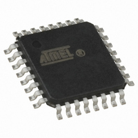
ATMEGA168-15AZ Atmel, ATMEGA168-15AZ Datasheet - Page 124

ATMEGA168-15AZ
Manufacturer Part Number
ATMEGA168-15AZ
Description
MCU AVR 16K FLASH 15MHZ 32-TQFP
Manufacturer
Atmel
Series
AVR® ATmegar
Datasheet
1.ATMEGA168-15AZ.pdf
(340 pages)
Specifications of ATMEGA168-15AZ
Package / Case
32-TQFP, 32-VQFP
Voltage - Supply (vcc/vdd)
2.7 V ~ 5.5 V
Operating Temperature
-40°C ~ 125°C
Speed
16MHz
Number Of I /o
23
Eeprom Size
512 x 8
Core Processor
AVR
Program Memory Type
FLASH
Ram Size
1K x 8
Program Memory Size
16KB (16K x 8)
Data Converters
A/D 8x10b
Oscillator Type
Internal
Peripherals
Brown-out Detect/Reset, POR, PWM, WDT
Connectivity
I²C, SPI, UART/USART
Core Size
8-Bit
Cpu Family
ATmega
Device Core
AVR
Device Core Size
8b
Frequency (max)
16MHz
Interface Type
2-Wire/USART/Serial
Total Internal Ram Size
1KB
# I/os (max)
23
Number Of Timers - General Purpose
3
Operating Supply Voltage (typ)
3.3/5V
Operating Supply Voltage (max)
5.5V
Operating Supply Voltage (min)
2.7V
On-chip Adc
8-chx10-bit
Instruction Set Architecture
RISC
Operating Temp Range
-40C to 125C
Operating Temperature Classification
Automotive
Mounting
Surface Mount
Pin Count
32
Package Type
TQFP
Lead Free Status / RoHS Status
Lead free / RoHS Compliant
Available stocks
Company
Part Number
Manufacturer
Quantity
Price
- Current page: 124 of 340
- Download datasheet (6Mb)
124
ATmega48/88/168 Automotive
Figure 14-9. Phase and Frequency Correct PWM Mode, Timing Diagram
The Timer/Counter Overflow Flag (TOV1) is set at the same timer clock cycle as the OCR1x
Registers are updated with the double buffer value (at BOTTOM). When either OCR1A or ICR1
is used for defining the TOP value, the OC1A or ICF1 Flag set when TCNT1 has reached TOP.
The Interrupt Flags can then be used to generate an interrupt each time the counter reaches the
TOP or BOTTOM value.
When changing the TOP value the program must ensure that the new TOP value is higher or
equal to the value of all of the Compare Registers. If the TOP value is lower than any of the
Compare Registers, a compare match will never occur between the TCNT1 and the OCR1x.
As
cal in all periods. Since the OCR1x Registers are updated at BOTTOM, the length of the rising
and the falling slopes will always be equal. This gives symmetrical output pulses and is therefore
frequency correct.
Using the ICR1 Register for defining TOP works well when using fixed TOP values. By using
ICR1, the OCR1A Register is free to be used for generating a PWM output on OC1A. However,
if the base PWM frequency is actively changed by changing the TOP value, using the OCR1A as
TOP is clearly a better choice due to its double buffer feature.
In phase and frequency correct PWM mode, the compare units allow generation of PWM wave-
forms on the OC1x pins. Setting the COM1x1:0 bits to two will produce a non-inverted PWM and
an inverted PWM output can be generated by setting the COM1x1:0 to three (See
page
port pin is set as output (DDR_OC1x). The PWM waveform is generated by setting (or clearing)
the OC1x Register at the compare match between OCR1x and TCNT1 when the counter incre-
ments, and clearing (or setting) the OC1x Register at compare match between OCR1x and
TCNT1 when the counter decrements. The PWM frequency for the output when using phase
and frequency correct PWM can be calculated by the following equation:
Figure 14-9
TCNTn
OCnx
OCnx
Period
128). The actual OC1x value will only be visible on the port pin if the data direction for the
shows the output generated is, in contrast to the phase correct mode, symmetri-
1
f
OCnxPFCPWM
2
=
3
---------------------------------
2
f
clk_I/O
N
TOP
4
OCnA Interrupt Flag Set
or ICFn Interrupt Flag Set
(Interrupt on TOP)
(COMnx1:0 = 2)
(COMnx1:0 = 3)
OCRnx/TOP Updateand
TOVn Interrupt Flag Set
(Interrupt on Bottom)
7530I–AVR–02/10
Table on
Related parts for ATMEGA168-15AZ
Image
Part Number
Description
Manufacturer
Datasheet
Request
R

Part Number:
Description:
Manufacturer:
Atmel Corporation
Datasheet:

Part Number:
Description:
Manufacturer:
Atmel Corporation
Datasheet:

Part Number:
Description:
Manufacturer:
ATMEL Corporation
Datasheet:

Part Number:
Description:
IC AVR MCU 16K 20MHZ 32TQFP
Manufacturer:
Atmel
Datasheet:

Part Number:
Description:
IC AVR MCU 16K 20MHZ 32-QFN
Manufacturer:
Atmel
Datasheet:

Part Number:
Description:
IC AVR MCU 16K 20MHZ 28DIP
Manufacturer:
Atmel
Datasheet:

Part Number:
Description:
MCU AVR 16K FLASH 15MHZ 32-QFN
Manufacturer:
Atmel
Datasheet:

Part Number:
Description:
IC AVR MCU 16K 20MHZ 32TQFP
Manufacturer:
Atmel
Datasheet:

Part Number:
Description:
MCU AVR 16KB FLASH 20MHZ 32QFN
Manufacturer:
Atmel
Datasheet:

Part Number:
Description:
MCU AVR 16KB FLASH 20MHZ 32TQFP
Manufacturer:
Atmel
Datasheet:

Part Number:
Description:
IC MCU AVR 16K FLASH 32-QFN
Manufacturer:
Atmel
Datasheet:


