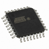
ATMEGA168-15AZ Atmel, ATMEGA168-15AZ Datasheet - Page 17

ATMEGA168-15AZ
Manufacturer Part Number
ATMEGA168-15AZ
Description
MCU AVR 16K FLASH 15MHZ 32-TQFP
Manufacturer
Atmel
Series
AVR® ATmegar
Datasheet
1.ATMEGA168-15AZ.pdf
(340 pages)
Specifications of ATMEGA168-15AZ
Package / Case
32-TQFP, 32-VQFP
Voltage - Supply (vcc/vdd)
2.7 V ~ 5.5 V
Operating Temperature
-40°C ~ 125°C
Speed
16MHz
Number Of I /o
23
Eeprom Size
512 x 8
Core Processor
AVR
Program Memory Type
FLASH
Ram Size
1K x 8
Program Memory Size
16KB (16K x 8)
Data Converters
A/D 8x10b
Oscillator Type
Internal
Peripherals
Brown-out Detect/Reset, POR, PWM, WDT
Connectivity
I²C, SPI, UART/USART
Core Size
8-Bit
Cpu Family
ATmega
Device Core
AVR
Device Core Size
8b
Frequency (max)
16MHz
Interface Type
2-Wire/USART/Serial
Total Internal Ram Size
1KB
# I/os (max)
23
Number Of Timers - General Purpose
3
Operating Supply Voltage (typ)
3.3/5V
Operating Supply Voltage (max)
5.5V
Operating Supply Voltage (min)
2.7V
On-chip Adc
8-chx10-bit
Instruction Set Architecture
RISC
Operating Temp Range
-40C to 125C
Operating Temperature Classification
Automotive
Mounting
Surface Mount
Pin Count
32
Package Type
TQFP
Lead Free Status / RoHS Status
Lead free / RoHS Compliant
Available stocks
Company
Part Number
Manufacturer
Quantity
Price
- Current page: 17 of 340
- Download datasheet (6Mb)
5.2.1
5.3
7530I–AVR–02/10
EEPROM Data Memory
Data Memory Access Times
Figure 5-3.
This section describes the general access timing concepts for internal memory access. The
internal data SRAM access is performed in two clk
Figure 5-4.
The ATmega48/88/168 contains 256/512/512 bytes of data EEPROM memory. It is organized
as a separate data space, in which single bytes can be read and written. The EEPROM has an
endurance of at least 100,000 write/erase cycles. The access between the EEPROM and the
CPU is described in the following, specifying the EEPROM Address Registers, the EEPROM
Data Register, and the EEPROM Control Register.
“Memory Programming” on page 278
in SPI or Parallel Programming mode.
Address
clk
Data Memory Map
On-chip Data SRAM Access Cycles
Data
Data
WR
CPU
RD
(512/1024/1024 x 8)
160 Ext I/O Reg.
64 I/O Registers
Data Memory
Compute Address
Internal SRAM
32 Registers
T1
Memory Access Instruction
contains a detailed description on EEPROM Programming
ATmega48/88/168 Automotive
0x02FF/0x04FF/0x04FF
0x0000 - 0x001F
0x0020 - 0x005F
0x0060 - 0x00FF
0x0100
Address valid
CPU
T2
cycles as described in
Next Instruction
T3
Figure
5-4.
17
Related parts for ATMEGA168-15AZ
Image
Part Number
Description
Manufacturer
Datasheet
Request
R

Part Number:
Description:
Manufacturer:
Atmel Corporation
Datasheet:

Part Number:
Description:
Manufacturer:
Atmel Corporation
Datasheet:

Part Number:
Description:
Manufacturer:
ATMEL Corporation
Datasheet:

Part Number:
Description:
IC AVR MCU 16K 20MHZ 32TQFP
Manufacturer:
Atmel
Datasheet:

Part Number:
Description:
IC AVR MCU 16K 20MHZ 32-QFN
Manufacturer:
Atmel
Datasheet:

Part Number:
Description:
IC AVR MCU 16K 20MHZ 28DIP
Manufacturer:
Atmel
Datasheet:

Part Number:
Description:
MCU AVR 16K FLASH 15MHZ 32-QFN
Manufacturer:
Atmel
Datasheet:

Part Number:
Description:
IC AVR MCU 16K 20MHZ 32TQFP
Manufacturer:
Atmel
Datasheet:

Part Number:
Description:
MCU AVR 16KB FLASH 20MHZ 32QFN
Manufacturer:
Atmel
Datasheet:

Part Number:
Description:
MCU AVR 16KB FLASH 20MHZ 32TQFP
Manufacturer:
Atmel
Datasheet:

Part Number:
Description:
IC MCU AVR 16K FLASH 32-QFN
Manufacturer:
Atmel
Datasheet:


