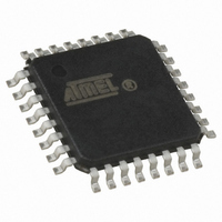
ATMEGA168-15AZ Atmel, ATMEGA168-15AZ Datasheet - Page 63

ATMEGA168-15AZ
Manufacturer Part Number
ATMEGA168-15AZ
Description
MCU AVR 16K FLASH 15MHZ 32-TQFP
Manufacturer
Atmel
Series
AVR® ATmegar
Datasheet
1.ATMEGA168-15AZ.pdf
(340 pages)
Specifications of ATMEGA168-15AZ
Package / Case
32-TQFP, 32-VQFP
Voltage - Supply (vcc/vdd)
2.7 V ~ 5.5 V
Operating Temperature
-40°C ~ 125°C
Speed
16MHz
Number Of I /o
23
Eeprom Size
512 x 8
Core Processor
AVR
Program Memory Type
FLASH
Ram Size
1K x 8
Program Memory Size
16KB (16K x 8)
Data Converters
A/D 8x10b
Oscillator Type
Internal
Peripherals
Brown-out Detect/Reset, POR, PWM, WDT
Connectivity
I²C, SPI, UART/USART
Core Size
8-Bit
Cpu Family
ATmega
Device Core
AVR
Device Core Size
8b
Frequency (max)
16MHz
Interface Type
2-Wire/USART/Serial
Total Internal Ram Size
1KB
# I/os (max)
23
Number Of Timers - General Purpose
3
Operating Supply Voltage (typ)
3.3/5V
Operating Supply Voltage (max)
5.5V
Operating Supply Voltage (min)
2.7V
On-chip Adc
8-chx10-bit
Instruction Set Architecture
RISC
Operating Temp Range
-40C to 125C
Operating Temperature Classification
Automotive
Mounting
Surface Mount
Pin Count
32
Package Type
TQFP
Lead Free Status / RoHS Status
Lead free / RoHS Compliant
Available stocks
Company
Part Number
Manufacturer
Quantity
Price
- Current page: 63 of 340
- Download datasheet (6Mb)
10.2
7530I–AVR–02/10
Ports as General Digital I/O
Figure 10-1. I/O Pin Equivalent Schematic
All registers and bit references in this section are written in general form. A lower case “x” repre-
sents the numbering letter for the port, and a lower case “n” represents the bit number. However,
when using the register or bit defines in a program, the precise form must be used. For example,
PORTB3 for bit no. 3 in Port B, here documented generally as PORTxn. The physical I/O Regis-
ters and bit locations are listed in
Three I/O memory address locations are allocated for each port, one each for the Data Register
– PORTx, Data Direction Register – DDRx, and the Port Input Pins – PINx. The Port Input Pins
I/O location is read only, while the Data Register and the Data Direction Register are read/write.
However, writing a logic one to a bit in the PINx Register, will result in a toggle in the correspond-
ing bit in the Data Register. In addition, the Pull-up Disable – PUD bit in MCUCR disables the
pull-up function for all pins in all ports when set.
Using the I/O port as General Digital I/O is described in
63. Most port pins are multiplexed with alternate functions for the peripheral features on the
device. How each alternate function interferes with the port pin is described in
Functions” on page
nate functions.
Note that enabling the alternate function of some of the port pins does not affect the use of the
other pins in the port as general digital I/O.
The ports are bi-directional I/O ports with optional internal pull-ups.
tional description of one I/O-port pin, here generically called Pxn.
Pxn
68. Refer to the individual module sections for a full description of the alter-
“Register Description for I/O Ports” on page
C
pin
ATmega48/88/168 Automotive
“Ports as General Digital I/O” on page
"General Digital I/O" for
See Figure
R
Details
pu
Figure 10-2
Logic
80.
“Alternate Port
shows a func-
63
Related parts for ATMEGA168-15AZ
Image
Part Number
Description
Manufacturer
Datasheet
Request
R

Part Number:
Description:
Manufacturer:
Atmel Corporation
Datasheet:

Part Number:
Description:
Manufacturer:
Atmel Corporation
Datasheet:

Part Number:
Description:
Manufacturer:
ATMEL Corporation
Datasheet:

Part Number:
Description:
IC AVR MCU 16K 20MHZ 32TQFP
Manufacturer:
Atmel
Datasheet:

Part Number:
Description:
IC AVR MCU 16K 20MHZ 32-QFN
Manufacturer:
Atmel
Datasheet:

Part Number:
Description:
IC AVR MCU 16K 20MHZ 28DIP
Manufacturer:
Atmel
Datasheet:

Part Number:
Description:
MCU AVR 16K FLASH 15MHZ 32-QFN
Manufacturer:
Atmel
Datasheet:

Part Number:
Description:
IC AVR MCU 16K 20MHZ 32TQFP
Manufacturer:
Atmel
Datasheet:

Part Number:
Description:
MCU AVR 16KB FLASH 20MHZ 32QFN
Manufacturer:
Atmel
Datasheet:

Part Number:
Description:
MCU AVR 16KB FLASH 20MHZ 32TQFP
Manufacturer:
Atmel
Datasheet:

Part Number:
Description:
IC MCU AVR 16K FLASH 32-QFN
Manufacturer:
Atmel
Datasheet:


