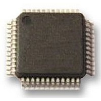
UPD78F0413GA-GAM-AX NEC, UPD78F0413GA-GAM-AX Datasheet - Page 509

UPD78F0413GA-GAM-AX
Manufacturer Part Number
UPD78F0413GA-GAM-AX
Description
8BIT UC, 32K FLASH, 1KB RAM, LCD
Manufacturer
NEC
Datasheet
1.UPD78F0413GA-GAM-AX.pdf
(562 pages)
Specifications of UPD78F0413GA-GAM-AX
Controller Family/series
UPD78F
No. Of I/o's
30
Ram Memory Size
1024Byte
Cpu Speed
10MHz
No. Of Timers
8
No. Of Pwm
RoHS Compliant
Core Size
8bit
Program Memory Size
32KB
Oscillator Type
External, Internal
Available stocks
Company
Part Number
Manufacturer
Quantity
Price
Company:
Part Number:
UPD78F0413GA-GAM-AX
Manufacturer:
ADI
Quantity:
882
Company:
Part Number:
UPD78F0413GA-GAM-AX
Manufacturer:
Renesas Electronics America
Quantity:
10 000
- Current page: 509 of 562
- Download datasheet (4Mb)
24.2 Writing with Flash memory programmer
(1) On-board programming
(2) Off-board programming
Notes 1.
Data can be written to the flash memory on-board or off-board, by using a dedicated flash memory programmer.
The contents of the flash memory can be rewritten after the 78K0/LC3 has been mounted on the target system.
The connectors that connect the dedicated flash memory programmer must be mounted on the target system.
Data can be written to the flash memory with a dedicated program adapter (FA series) before the 78K0/LC3 is
mounted on the target system.
2.
3.
Remark The FA series is a product of Naito Densei Machida Mfg. Co., Ltd.
Only the X1 clock (f
using the clock output of the dedicated flash memory programmer, pin connection varies depending on the
type of the dedicated flash memory programmer used.
PD78F040x only.
PD78F041x only.
PG-FP4, FL-PR4:
PG-FPL3, FP-LITE3:
Table 24-2. Wiring Between 78K0/LC3 and Dedicated Flash memory programmer
Pin Configuration of Dedicated Flash memory programmer
SI/RxD
SO/TxD
SCK
CLK
/RESET
FLMD0
V
GND
Signal Name
DD
X
Input
Output
Output
Output
Output
Output
I/O
) or external main system clock (f
I/O
Connect CLK of the programmer to EXCLK/X2/P122 (pin 10).
Connect CLK of the programmer to X1/P121 (pin 11), and connect its inverted
signal to X2/EXCLK/P122 (pin 10).
CHAPTER 24 FLASH MEMORY
Receive signal
Transmit signal
Transfer clock
Clock to 78K0/LC3
Reset signal
Mode signal
V
power monitoring
Ground
DD
User’s Manual U18698EJ1V0UD
voltage generation/
Pin Function
EXCLK
TxD6/SEG6/P112
RxD6/SEG7/P113
RESET
FLMD0
V
V
AV
V
V
AV
DD
DD
SS
SS
REF
SS
Note 2
Note 2
) can be used when UART6 is used. When
Note 3
Note 3
Pin Name
Note 1
With UART6
Pin No.
Note 1
24
23
14
35
13
36
6
9
509
Related parts for UPD78F0413GA-GAM-AX
Image
Part Number
Description
Manufacturer
Datasheet
Request
R

Part Number:
Description:
16/8 bit single-chip microcomputer
Manufacturer:
NEC
Datasheet:

Part Number:
Description:
Dual audio power amp circuit
Manufacturer:
NEC
Datasheet:

Part Number:
Description:
Dual comparator
Manufacturer:
NEC
Datasheet:

Part Number:
Description:
MOS type composite field effect transistor
Manufacturer:
NEC
Datasheet:

Part Number:
Description:
50 V/100 mA FET array incorporating 2 N-ch MOSFETs
Manufacturer:
NEC
Datasheet:

Part Number:
Description:
6-pin small MM high-frequency double transistor
Manufacturer:
NEC
Datasheet:

Part Number:
Description:
6-pin small MM high-frequency double transistor
Manufacturer:
NEC
Datasheet:

Part Number:
Description:
6-pin small MM high-frequency double transistor
Manufacturer:
NEC
Datasheet:

Part Number:
Description:
6-pin small MM high-frequency double transistor
Manufacturer:
NEC
Datasheet:

Part Number:
Description:
Twin transistors equipped with different model chips(6P small MM)
Manufacturer:
NEC
Datasheet:

Part Number:
Description:
Bipolar analog integrated circuit
Manufacturer:
NEC
Datasheet:


