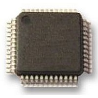
UPD78F0413GA-GAM-AX NEC, UPD78F0413GA-GAM-AX Datasheet - Page 324

UPD78F0413GA-GAM-AX
Manufacturer Part Number
UPD78F0413GA-GAM-AX
Description
8BIT UC, 32K FLASH, 1KB RAM, LCD
Manufacturer
NEC
Datasheet
1.UPD78F0413GA-GAM-AX.pdf
(562 pages)
Specifications of UPD78F0413GA-GAM-AX
Controller Family/series
UPD78F
No. Of I/o's
30
Ram Memory Size
1024Byte
Cpu Speed
10MHz
No. Of Timers
8
No. Of Pwm
RoHS Compliant
Core Size
8bit
Program Memory Size
32KB
Oscillator Type
External, Internal
Available stocks
Company
Part Number
Manufacturer
Quantity
Price
Company:
Part Number:
UPD78F0413GA-GAM-AX
Manufacturer:
ADI
Quantity:
882
Company:
Part Number:
UPD78F0413GA-GAM-AX
Manufacturer:
Renesas Electronics America
Quantity:
10 000
- Current page: 324 of 562
- Download datasheet (4Mb)
13.4.2 Asynchronous serial interface (UART) mode
baud rates.
(1) Registers used
324
POWER0 TXE0
In this mode, 1-byte data is transmitted/received following a start bit, and a full-duplex operation can be performed.
A dedicated UART baud rate generator is incorporated, so that communication can be executed at a wide range of
Note Can be set as port function, key interrupt, or serial interface UART6 (only when UART0 is stopped).
Remarks 1.
0
1
<1> Set the BRGC0 register (see Figure 13-4).
<2> Set bits 1 to 4 (SL0, CL0, PS00, and PS01) of the ASIM0 register (see Figure 13-2).
<3> Set bit 7 (POWER0) of the ASIM0 register to 1.
<4> Set bit 6 (TXE0) of the ASIM0 register to 1.
<5> Write data to the TXS0 register.
The basic procedure of setting an operation in the UART mode is as follows.
Caution Take relationship with the other party of communication when setting the port mode register
The relationship between the register settings and pins is shown below.
Asynchronous serial interface operation mode register 0 (ASIM0)
Asynchronous serial interface reception error status register 0 (ASIS0)
Baud rate generator control register 0 (BRGC0)
Port mode register 1 (PM1)
Port register 1 (P1)
Set bit 5 (RXE0) of the ASIM0 register to 1.
0
0
1
1
2.
and port register.
POWER0: Bit 7 of asynchronous serial interface operation mode register 0 (ASIM0)
TXE0:
RXE0:
PM1 :
P1 :
The functions within arrowheads (< >) can be assigned by setting the input switch control register
(ISC).
:
RXE0
0
1
0
1
Table 13-2. Relationship Between Register Settings and Pins
PM13
Note
Note
0
0
don’t care
Bit 6 of ASIM0
Bit 5 of ASIM0
Port mode register
Port output latch
P13
CHAPTER 13 SERIAL INTERFACE UART0
Note
Note
PM12
Data transmission is started.
User’s Manual U18698EJ1V0UD
Note
Note
1
1
P12
Note
Note
Transmission is enabled.
Reception is enabled.
Transmission/
Transmission
Reception
Operation
reception
UART0
Stop
TxD0/KR4/P13/<TxD6> RxD0/KR3/P12/<RxD6>
KR4/P13/<TxD6>
KR4/P13
TxD0
TxD0
Pin Function
KR3/P12/<RxD6>
KR3/P12
RxD0
RxD0
Related parts for UPD78F0413GA-GAM-AX
Image
Part Number
Description
Manufacturer
Datasheet
Request
R

Part Number:
Description:
16/8 bit single-chip microcomputer
Manufacturer:
NEC
Datasheet:

Part Number:
Description:
Dual audio power amp circuit
Manufacturer:
NEC
Datasheet:

Part Number:
Description:
Dual comparator
Manufacturer:
NEC
Datasheet:

Part Number:
Description:
MOS type composite field effect transistor
Manufacturer:
NEC
Datasheet:

Part Number:
Description:
50 V/100 mA FET array incorporating 2 N-ch MOSFETs
Manufacturer:
NEC
Datasheet:

Part Number:
Description:
6-pin small MM high-frequency double transistor
Manufacturer:
NEC
Datasheet:

Part Number:
Description:
6-pin small MM high-frequency double transistor
Manufacturer:
NEC
Datasheet:

Part Number:
Description:
6-pin small MM high-frequency double transistor
Manufacturer:
NEC
Datasheet:

Part Number:
Description:
6-pin small MM high-frequency double transistor
Manufacturer:
NEC
Datasheet:

Part Number:
Description:
Twin transistors equipped with different model chips(6P small MM)
Manufacturer:
NEC
Datasheet:

Part Number:
Description:
Bipolar analog integrated circuit
Manufacturer:
NEC
Datasheet:


