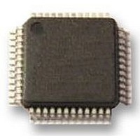
UPD78F0413GA-GAM-AX NEC, UPD78F0413GA-GAM-AX Datasheet - Page 343

UPD78F0413GA-GAM-AX
Manufacturer Part Number
UPD78F0413GA-GAM-AX
Description
8BIT UC, 32K FLASH, 1KB RAM, LCD
Manufacturer
NEC
Datasheet
1.UPD78F0413GA-GAM-AX.pdf
(562 pages)
Specifications of UPD78F0413GA-GAM-AX
Controller Family/series
UPD78F
No. Of I/o's
30
Ram Memory Size
1024Byte
Cpu Speed
10MHz
No. Of Timers
8
No. Of Pwm
RoHS Compliant
Core Size
8bit
Program Memory Size
32KB
Oscillator Type
External, Internal
Available stocks
Company
Part Number
Manufacturer
Quantity
Price
Company:
Part Number:
UPD78F0413GA-GAM-AX
Manufacturer:
ADI
Quantity:
882
Company:
Part Number:
UPD78F0413GA-GAM-AX
Manufacturer:
Renesas Electronics America
Quantity:
10 000
- Current page: 343 of 562
- Download datasheet (4Mb)
Note If “reception as 0 parity” is selected, the parity is not judged. Therefore, bit 2 (PE6) of asynchronous serial
Cautions 1. To start the transmission, set POWER6 to 1 and then set TXE6 to 1. To stop the transmission,
Figure 14-5. Format of Asynchronous Serial Interface Operation Mode Register 6 (ASIM6) (2/2)
interface reception error status register 6 (ASIS6) is not set and the error interrupt does not occur.
2. To start the reception, set POWER6 to 1 and then set RXE6 to 1. To stop the reception, clear
3. Set POWER6 to 1 and then set RXE6 to 1 while a high level is input to the R
4. TXE6 and RXE6 are synchronized by the base clock (f
5. Set transmit data to TXB6 at least one base clock (f
6. Clear the TXE6 and RXE6 bits to 0 before rewriting the PS61, PS60, and CL6 bits.
7. Fix the PS61 and PS60 bits to 0 when used in LIN communication operation.
8. Clear TXE6 to 0 before rewriting the SL6 bit.
9. Make sure that RXE6 = 0 when rewriting the ISRM6 bit.
ISRM6
PS61
clear TXE6 to 0, and then clear POWER6 to 0.
RXE6 to 0, and then clear POWER6 to 0.
POWER6 is set to 1 and RXE6 is set to 1 while a low level is input, reception is started.
transmission or reception again, set TXE6 or RXE6 to 1 at least two clocks of the base clock
after TXE6 or RXE6 has been cleared to 0. If TXE6 or RXE6 is set within two clocks of the
base clock, the transmission circuit or reception circuit may not be initialized.
number of stop bits = 1”, and therefore, is not affected by the set value of the SL6 bit.
CL6
SL6
0
0
1
1
0
1
0
1
0
1
Character length of data = 7 bits
Character length of data = 8 bits
Number of stop bits = 1
Number of stop bits = 2
“INTSRE6” occurs in case of error (at this time, INTSR6 does not occur).
“INTSR6” occurs in case of error (at this time, INTSRE6 does not occur).
PS60
0
1
0
1
Enables/disables occurrence of reception completion interrupt in case of error
CHAPTER 14 SERIAL INTERFACE UART6
Does not output parity bit.
Outputs 0 parity.
Outputs odd parity.
Outputs even parity.
User’s Manual U18698EJ1V0UD
Transmission operation
Specifies character length of transmit/receive data
Specifies number of stop bits of transmit data
Reception is always performed with “the
XCLK6
) after setting TXE6 = 1.
Reception without parity
Reception as 0 parity
Judges as odd parity.
Judges as even parity.
XCLK6
) set by CKSR6.
Reception operation
Note
X
D6 pin. If
To enable
343
Related parts for UPD78F0413GA-GAM-AX
Image
Part Number
Description
Manufacturer
Datasheet
Request
R

Part Number:
Description:
16/8 bit single-chip microcomputer
Manufacturer:
NEC
Datasheet:

Part Number:
Description:
Dual audio power amp circuit
Manufacturer:
NEC
Datasheet:

Part Number:
Description:
Dual comparator
Manufacturer:
NEC
Datasheet:

Part Number:
Description:
MOS type composite field effect transistor
Manufacturer:
NEC
Datasheet:

Part Number:
Description:
50 V/100 mA FET array incorporating 2 N-ch MOSFETs
Manufacturer:
NEC
Datasheet:

Part Number:
Description:
6-pin small MM high-frequency double transistor
Manufacturer:
NEC
Datasheet:

Part Number:
Description:
6-pin small MM high-frequency double transistor
Manufacturer:
NEC
Datasheet:

Part Number:
Description:
6-pin small MM high-frequency double transistor
Manufacturer:
NEC
Datasheet:

Part Number:
Description:
6-pin small MM high-frequency double transistor
Manufacturer:
NEC
Datasheet:

Part Number:
Description:
Twin transistors equipped with different model chips(6P small MM)
Manufacturer:
NEC
Datasheet:

Part Number:
Description:
Bipolar analog integrated circuit
Manufacturer:
NEC
Datasheet:


