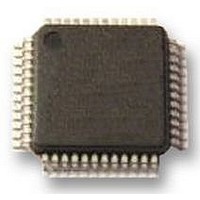
UPD78F0413GA-GAM-AX NEC, UPD78F0413GA-GAM-AX Datasheet - Page 190

UPD78F0413GA-GAM-AX
Manufacturer Part Number
UPD78F0413GA-GAM-AX
Description
8BIT UC, 32K FLASH, 1KB RAM, LCD
Manufacturer
NEC
Datasheet
1.UPD78F0413GA-GAM-AX.pdf
(562 pages)
Specifications of UPD78F0413GA-GAM-AX
Controller Family/series
UPD78F
No. Of I/o's
30
Ram Memory Size
1024Byte
Cpu Speed
10MHz
No. Of Timers
8
No. Of Pwm
RoHS Compliant
Core Size
8bit
Program Memory Size
32KB
Oscillator Type
External, Internal
Available stocks
Company
Part Number
Manufacturer
Quantity
Price
Company:
Part Number:
UPD78F0413GA-GAM-AX
Manufacturer:
ADI
Quantity:
882
Company:
Part Number:
UPD78F0413GA-GAM-AX
Manufacturer:
Renesas Electronics America
Quantity:
10 000
- Current page: 190 of 562
- Download datasheet (4Mb)
6.4.6 PPG output operation
(Programmable Pulse Generator) signal during a cycle set by CR000 when bits 3 and 2 (TMC003 and TMC002) of 16-
bit timer mode control register 00 (TMC00) are set to 11 (clear & start upon a match between TM00 and CR000).
190
A square wave having a pulse width set in advance by CR010 is output from the TO00 pin as a PPG
The pulse cycle and duty factor of the pulse generated as the PPG output are as follows.
Caution To change the duty factor (value of CR010) during operation, see 6.5.1 Rewriting CR010 during
Remarks 1. For the setting of I/O pins, see 6.3 (6) Port mode register 3 (PM3).
Pulse cycle = (Set value of CR000 + 1)
Duty = (Set value of CR010 + 1) / (Set value of CR000 + 1)
Count clock
TM00 operation.
2. For how to enable the INTTM000 signal interrupt, see CHAPTER 17 INTERRUPT FUNCTIONS.
TMC003, TMC002
Operable bits
Figure 6-41. Block Diagram of PPG Output Operation
CHAPTER 6 16-BIT TIMER/EVENT COUNTER 00
User’s Manual U18698EJ1V0UD
Count clock cycle
Compare register
Timer counter
Match signal
(CR010)
(TM00)
Compare register
Clear
(CR000)
Match signal
controller
Output
TO00
output
Interrupt signal
(INTTM000)
Interrupt signal
(INTTM010)
TO00 pin
Related parts for UPD78F0413GA-GAM-AX
Image
Part Number
Description
Manufacturer
Datasheet
Request
R

Part Number:
Description:
16/8 bit single-chip microcomputer
Manufacturer:
NEC
Datasheet:

Part Number:
Description:
Dual audio power amp circuit
Manufacturer:
NEC
Datasheet:

Part Number:
Description:
Dual comparator
Manufacturer:
NEC
Datasheet:

Part Number:
Description:
MOS type composite field effect transistor
Manufacturer:
NEC
Datasheet:

Part Number:
Description:
50 V/100 mA FET array incorporating 2 N-ch MOSFETs
Manufacturer:
NEC
Datasheet:

Part Number:
Description:
6-pin small MM high-frequency double transistor
Manufacturer:
NEC
Datasheet:

Part Number:
Description:
6-pin small MM high-frequency double transistor
Manufacturer:
NEC
Datasheet:

Part Number:
Description:
6-pin small MM high-frequency double transistor
Manufacturer:
NEC
Datasheet:

Part Number:
Description:
6-pin small MM high-frequency double transistor
Manufacturer:
NEC
Datasheet:

Part Number:
Description:
Twin transistors equipped with different model chips(6P small MM)
Manufacturer:
NEC
Datasheet:

Part Number:
Description:
Bipolar analog integrated circuit
Manufacturer:
NEC
Datasheet:


