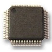
UPD78F0413GA-GAM-AX NEC, UPD78F0413GA-GAM-AX Datasheet - Page 436

UPD78F0413GA-GAM-AX
Manufacturer Part Number
UPD78F0413GA-GAM-AX
Description
8BIT UC, 32K FLASH, 1KB RAM, LCD
Manufacturer
NEC
Datasheet
1.UPD78F0413GA-GAM-AX.pdf
(562 pages)
Specifications of UPD78F0413GA-GAM-AX
Controller Family/series
UPD78F
No. Of I/o's
30
Ram Memory Size
1024Byte
Cpu Speed
10MHz
No. Of Timers
8
No. Of Pwm
RoHS Compliant
Core Size
8bit
Program Memory Size
32KB
Oscillator Type
External, Internal
Available stocks
Company
Part Number
Manufacturer
Quantity
Price
Company:
Part Number:
UPD78F0413GA-GAM-AX
Manufacturer:
ADI
Quantity:
882
Company:
Part Number:
UPD78F0413GA-GAM-AX
Manufacturer:
Renesas Electronics America
Quantity:
10 000
- Current page: 436 of 562
- Download datasheet (4Mb)
436
Maskable
Interrupt
Notes 1.
Type
2.
3.
4.
5.
Priority
Default
The default priority determines the sequence of processing vectored interrupts if two or more maskable
interrupts occur simultaneously. Zero indicates the highest priority and 22 indicates the lowest priority.
Basic configuration types (A) to (D) correspond to (A) to (D) in Figure 17-1.
When bit 1 (LVIMD) of the low-voltage detection register (LVIM) is cleared to 0.
When 8-bit timer/event counter 51 and 8-bit timer H1 are used in the carrier generator mode, an
interrupt is generated upon the timing when the INTTM5H1 signal is generated (see Figure 8-15
Transfer Timing).
10
11
12
13
14
15
16
17
18
19
PD78F041x only.
0
1
2
3
4
5
6
7
8
9
Note 1
INTLVI
INTP0
INTP1
INTP2
INTP3
INTSRE6
INTSR6
INTST6
INTST0
INTTMH1
INTTMH0
INTTM50
INTTM000
INTTM010
INTAD
INTSR0
INTRTC
INTTM51
Note 4
INTKR
INTRTCI
Name
Note 5
Low-voltage detection
Pin input edge detection
UART6 reception error generation
End of UART6 reception
End of UART6 transmission
End of UART0 transmission
Match between TMH1 and CMP01
(when compare register is specified)
Match between TMH0 and CMP00
(when compare register is specified)
Match between TM50 and CR50
(when compare register is specified)
Match between TM00 and CR000
(when compare register is specified),
TI010 pin valid edge detection
(when capture register is specified)
Match between TM00 and CR010
(when compare register is specified),
TI000 pin valid edge detection
(when capture register is specified)
End of 10-bit successive approximation type
A/D conversion
End of UART0 reception or reception error
generation
Fixed-cycle signal of real-time counter/alarm
match detection
Match between TM51 and CR51
(when compare register is specified)
Key interrupt detection
Interval signal detection of real-time counter
Table 17-1. Interrupt Source List (1/2)
CHAPTER 17 INTERRUPT FUNCTIONS
Interrupt Source
User’s Manual U18698EJ1V0UD
Trigger
Note 3
Internal
External
Internal
External
Internal
Internal/
External
Address
000AH
000CH
001AH
001CH
001EH
002AH
002CH
002EH
0004H
0006H
0008H
0012H
0014H
0016H
0018H
0020H
0022H
0024H
0026H
0028H
Vector
Table
Configuration
Type
Basic
(C)
(A)
(B)
(A)
(A)
Note 2
Related parts for UPD78F0413GA-GAM-AX
Image
Part Number
Description
Manufacturer
Datasheet
Request
R

Part Number:
Description:
16/8 bit single-chip microcomputer
Manufacturer:
NEC
Datasheet:

Part Number:
Description:
Dual audio power amp circuit
Manufacturer:
NEC
Datasheet:

Part Number:
Description:
Dual comparator
Manufacturer:
NEC
Datasheet:

Part Number:
Description:
MOS type composite field effect transistor
Manufacturer:
NEC
Datasheet:

Part Number:
Description:
50 V/100 mA FET array incorporating 2 N-ch MOSFETs
Manufacturer:
NEC
Datasheet:

Part Number:
Description:
6-pin small MM high-frequency double transistor
Manufacturer:
NEC
Datasheet:

Part Number:
Description:
6-pin small MM high-frequency double transistor
Manufacturer:
NEC
Datasheet:

Part Number:
Description:
6-pin small MM high-frequency double transistor
Manufacturer:
NEC
Datasheet:

Part Number:
Description:
6-pin small MM high-frequency double transistor
Manufacturer:
NEC
Datasheet:

Part Number:
Description:
Twin transistors equipped with different model chips(6P small MM)
Manufacturer:
NEC
Datasheet:

Part Number:
Description:
Bipolar analog integrated circuit
Manufacturer:
NEC
Datasheet:


