ATEVK1104 Atmel, ATEVK1104 Datasheet - Page 752
ATEVK1104
Manufacturer Part Number
ATEVK1104
Description
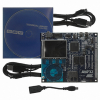
KIT DEV/EVAL FOR AVR32 AT32UC3A
Manufacturer
Atmel
Series
AVR®32r
Type
MCUr
Datasheets
1.ATAVRONE-PROBECBL.pdf
(16 pages)
2.ATEVK1104.pdf
(826 pages)
3.ATEVK1104.pdf
(90 pages)
4.ATEVK1104.pdf
(6 pages)
5.ATEVK1104.pdf
(12 pages)
Specifications of ATEVK1104
Contents
Evaluation Board, Software and Documentation
Processor To Be Evaluated
AT32UC3A3
Data Bus Width
32 bit
Interface Type
USB, SPI, USART
Silicon Manufacturer
Atmel
Core Architecture
AVR
Core Sub-architecture
AVR UC3
Silicon Core Number
AT32UC3A3256
Silicon Family Name
AVR
Kit Contents
Board CD Docs
Rohs Compliant
Yes
For Use With/related Products
AT32UC3A3
Lead Free Status / RoHS Status
Lead free / RoHS Compliant
Available stocks
Company
Part Number
Manufacturer
Quantity
Price
Company:

Part Number:
ATEVK1104
Manufacturer:
Atmel
Quantity:
135


36.9.3
32058J–AVR32–04/11
MEMORY_SERVICE
For any operation, the full 7 bits of the address must be provided. For write operations, 32 data
bits must be provided, or the result will be undefined. For read operations, shifting may be termi-
nated once the required number of bits have been acquired.
Table 36-5.
This instruction allows access to registers in an optional Memory Service unit. Memory Service
registers are addressed by their register index, as listed in the Memory Service documentation.
The 7-bit register index and a read/write control bit, and the 32-bit data is accessed through the
JTAG port.
The Memory Service unit may offer features such as CRC calculation of memory, debug trace
support, and test features. Please refer to the Memory Service Unit documentation and the part
specific documentation for details.
The data register is alternately interpreted by the SAB as an address register and a data regis-
ter. The SAB starts in address mode after the MEMORY_SERVICE instruction is selected, and
toggles between address and data mode each time a data scan completes with the busy bit
cleared.
Starting in Run-Test/Idle, Memory Service registers are accessed in the following way:
Instructions
IR input value
IR output value
DR Size
DR input value (Address phase)
DR input value (Data read phase)
DR input value (Data write phase)
DR output value (Address phase)
DR output value (Data read phase)
DR output value (Data write phase)
1. Select the DR Scan path.
2. Scan in the 7-bit address for the Memory Service register and a direction bit (1=read,
3. Go to Update-DR and re-enter Select-DR Scan.
4. For a read operation, scan out the contents of the addressed register. For a write oper-
5. Return to Run-Test/Idle.
0=write).
ation, scan in the new contents of the register.
NEXUS_ACCESS details
Details
10000 (0x10)
peb01
34 bits
aaaaaaar xxxxxxxx xxxxxxxx xxxxxxxx xx
xxxxxxxx xxxxxxxx xxxxxxxx xxxxxxxx xx
dddddddd dddddddd dddddddd dddddddd xx
xx xxxxxxxx xxxxxxxx xxxxxxxx xxxxxxeb
eb dddddddd dddddddd dddddddd dddddddd
xx xxxxxxxx xxxxxxxx xxxxxxxx xxxxxxeb
AT32UC3A
752
Related parts for ATEVK1104
Image
Part Number
Description
Manufacturer
Datasheet
Request
R

Part Number:
Description:
DEV KIT FOR AVR/AVR32
Manufacturer:
Atmel
Datasheet:

Part Number:
Description:
INTERVAL AND WIPE/WASH WIPER CONTROL IC WITH DELAY
Manufacturer:
ATMEL Corporation
Datasheet:
Part Number:
Description:
Low-Voltage Voice-Switched IC for Hands-Free Operation
Manufacturer:
ATMEL Corporation
Datasheet:
Part Number:
Description:
MONOLITHIC INTEGRATED FEATUREPHONE CIRCUIT
Manufacturer:
ATMEL Corporation
Datasheet:
Part Number:
Description:
AM-FM Receiver IC U4255BM-M
Manufacturer:
ATMEL Corporation
Datasheet:
Part Number:
Description:
Monolithic Integrated Feature Phone Circuit
Manufacturer:
ATMEL Corporation
Datasheet:
Part Number:
Description:
Multistandard Video-IF and Quasi Parallel Sound Processing
Manufacturer:
ATMEL Corporation
Datasheet:
Part Number:
Description:
High-performance EE PLD
Manufacturer:
ATMEL Corporation
Datasheet:
Part Number:
Description:
8-bit Flash Microcontroller
Manufacturer:
ATMEL Corporation
Datasheet:
Part Number:
Description:
2-Wire Serial EEPROM
Manufacturer:
ATMEL Corporation
Datasheet: