ATEVK1104 Atmel, ATEVK1104 Datasheet - Page 747
ATEVK1104
Manufacturer Part Number
ATEVK1104
Description
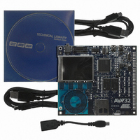
KIT DEV/EVAL FOR AVR32 AT32UC3A
Manufacturer
Atmel
Series
AVR®32r
Type
MCUr
Datasheets
1.ATAVRONE-PROBECBL.pdf
(16 pages)
2.ATEVK1104.pdf
(826 pages)
3.ATEVK1104.pdf
(90 pages)
4.ATEVK1104.pdf
(6 pages)
5.ATEVK1104.pdf
(12 pages)
Specifications of ATEVK1104
Contents
Evaluation Board, Software and Documentation
Processor To Be Evaluated
AT32UC3A3
Data Bus Width
32 bit
Interface Type
USB, SPI, USART
Silicon Manufacturer
Atmel
Core Architecture
AVR
Core Sub-architecture
AVR UC3
Silicon Core Number
AT32UC3A3256
Silicon Family Name
AVR
Kit Contents
Board CD Docs
Rohs Compliant
Yes
For Use With/related Products
AT32UC3A3
Lead Free Status / RoHS Status
Lead free / RoHS Compliant
Available stocks
Company
Part Number
Manufacturer
Quantity
Price
Company:

Part Number:
ATEVK1104
Manufacturer:
Atmel
Quantity:
135


36.6.4.2
36.6.5
32058J–AVR32–04/11
Memory programming
Error reporting
What to do if the busy bit is set:
The Service access port may not be able to complete all accesses as requested. This may be
because the address is invalid, the addressed area is read-only or cannot handle byte/halfword
accesses, or because the chip is set in a protected mode where only limited accesses are
allowed.
The error bit is updated when an access completes, and is cleared when a new access starts.
What to do if the error bit is set:
The High-Speed Bus (HSB) in the device is mapped as a slave on the SAB. This enables all
HSB-mapped memories to be read or written through the SAB using JTAG instructions, as
described in
Internal SRAM can always be directly accessed. External static memory or SDRAM can be
accessed if the EBI has been correctly configured to access this memory. It is also possible to
access the configuration registers for these modules to set up the correct configuration. Simi-
larly, external parallel flash can be programmed by accessing the registers for the flash device
through the EBI.
The internal flash and fuses can likewise be programmed by accessing the registers in the Flash
Controller. When the security fuse is set, access to internal memory is blocked, and the
CHIP_ERASE instruction must be used to erase the fuse and flash contents. For detail see the
SAB address map section.
• A SYNC countdown completed.
• A operation is cancelled by the CANCEL_ACCESS instruction.
• During Shift-IR: The new instruction is selected, but the previous operation has not yet
• During Shift-DR of an address: The new address is ignored. The SAB stays in address mode,
• During Shift-DR of read data: The read data are invalid. The SAB stays in data mode. Repeat
• During Shift-DR of write data: The write data are ignored. The SAB stays in data mode.
• During Shift-IR: The new instruction is selected. The last operation performed using the old
• During Shift-DR of an address: The previous operation failed. The new address is accepted.
• During Shift-DR of read data: The read operation failed, and the read data are invalid.
• During Shift-DR of write data: The previous write operation failed. The new data are accepted
• While polling with CANCEL_ACCESS: The previous access was cancelled. It may or may not
completed and will continue (unless the new instruction is CANCEL_ACCESS). You may
continue shifting the same instruction until the busy bit clears, or start shifting data. If shifting
data, you must be prepared that the data shift may also report busy.
so no data must be shifted. Repeat the address until the busy bit clears.
scanning until the busy bit clears.
Repeat scanning until the busy bit clears.
instruction did not complete successfully.
If the read bit is set, a read operation is started.
and a write operation started. This should only occur during block writes or stream writes. No
error can occur between scanning a write address and the following write data.
have actually completed.
Section
36.6.4.
AT32UC3A
747
Related parts for ATEVK1104
Image
Part Number
Description
Manufacturer
Datasheet
Request
R

Part Number:
Description:
DEV KIT FOR AVR/AVR32
Manufacturer:
Atmel
Datasheet:

Part Number:
Description:
INTERVAL AND WIPE/WASH WIPER CONTROL IC WITH DELAY
Manufacturer:
ATMEL Corporation
Datasheet:
Part Number:
Description:
Low-Voltage Voice-Switched IC for Hands-Free Operation
Manufacturer:
ATMEL Corporation
Datasheet:
Part Number:
Description:
MONOLITHIC INTEGRATED FEATUREPHONE CIRCUIT
Manufacturer:
ATMEL Corporation
Datasheet:
Part Number:
Description:
AM-FM Receiver IC U4255BM-M
Manufacturer:
ATMEL Corporation
Datasheet:
Part Number:
Description:
Monolithic Integrated Feature Phone Circuit
Manufacturer:
ATMEL Corporation
Datasheet:
Part Number:
Description:
Multistandard Video-IF and Quasi Parallel Sound Processing
Manufacturer:
ATMEL Corporation
Datasheet:
Part Number:
Description:
High-performance EE PLD
Manufacturer:
ATMEL Corporation
Datasheet:
Part Number:
Description:
8-bit Flash Microcontroller
Manufacturer:
ATMEL Corporation
Datasheet:
Part Number:
Description:
2-Wire Serial EEPROM
Manufacturer:
ATMEL Corporation
Datasheet: