ATEVK1104 Atmel, ATEVK1104 Datasheet - Page 509
ATEVK1104
Manufacturer Part Number
ATEVK1104
Description
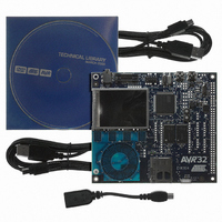
KIT DEV/EVAL FOR AVR32 AT32UC3A
Manufacturer
Atmel
Series
AVR®32r
Type
MCUr
Datasheets
1.ATAVRONE-PROBECBL.pdf
(16 pages)
2.ATEVK1104.pdf
(826 pages)
3.ATEVK1104.pdf
(90 pages)
4.ATEVK1104.pdf
(6 pages)
5.ATEVK1104.pdf
(12 pages)
Specifications of ATEVK1104
Contents
Evaluation Board, Software and Documentation
Processor To Be Evaluated
AT32UC3A3
Data Bus Width
32 bit
Interface Type
USB, SPI, USART
Silicon Manufacturer
Atmel
Core Architecture
AVR
Core Sub-architecture
AVR UC3
Silicon Core Number
AT32UC3A3256
Silicon Family Name
AVR
Kit Contents
Board CD Docs
Rohs Compliant
Yes
For Use With/related Products
AT32UC3A3
Lead Free Status / RoHS Status
Lead free / RoHS Compliant
Available stocks
Company
Part Number
Manufacturer
Quantity
Price
Company:

Part Number:
ATEVK1104
Manufacturer:
Atmel
Quantity:
135


30.7.1.8
Table 30-4.
30.7.1.9
Figure 30-11. Plug-In Detection Input Block Diagram
32058J–AVR32–04/11
00b
01b
10b
11b
Plug-In Detection
Customizing of OTG Timers
([OTG] Chapter 6.6.5.1)
Customizing of OTG Timers
AWaitVrise Time-Out
VBUS
100 ms
20 ms
50 ms
70 ms
00b:
It is possible to refine some OTG timers thanks to the TIMPAGE and TIMVALUE bit-fields, as
shown by
TIMPAGE is used to select the OTG timer to access while TIMVALUE indicates the time-out
value of the selected timer.
TIMPAGE and TIMVALUE can be read or written. Before writing them, the firmware should
unlock write accesses by setting the UNLOCK bit. This is not required for read accesses, except
before accessing TIMPAGE if it has to be written in order to read the TIMVALUE bit-field of
another OTG timer.
The USB connection is detected from the VBUS pad.
plug-in detector.
The control logic of the VBUS pad outputs two signals:
In device mode, the VBUS bit follows the Session_valid comparator output:
•the Session_valid signal is high when the voltage on the VBUS pad is higher than or equal to
•the Va_Vbus_valid signal is high when the voltage on the VBUS pad is higher than or equal to
•it is set when the voltage on the VBUS pad is higher than or equal to 1.4 V;
1.4 V;
4.4 V.
Pad Logic
Figure
VDD
GND
VbBusPulsing Time-Out
([OTG] Chapter 5.3.4)
30-4.
Session_valid
Va_Vbus_valid
VBus_pulsing
VBus_discharge
23 ms
31 ms
40 ms
15 ms
01b:
Logic
TIMPAGE
PdTmOutCnt Time-Out
([OTG] Chapter 5.3.2)
USBSTA
VBUS
105 ms
118 ms
131 ms
93 ms
10b:
Figure 30-11
VBUSTI
USBSTA
shows the architecture of the
SRPDetTmOut Time-Out
([OTG] Chapter 5.3.3)
AT32UC3A
100 µs
11 ms
10 µs
1 ms
11b:
509
Related parts for ATEVK1104
Image
Part Number
Description
Manufacturer
Datasheet
Request
R

Part Number:
Description:
DEV KIT FOR AVR/AVR32
Manufacturer:
Atmel
Datasheet:

Part Number:
Description:
INTERVAL AND WIPE/WASH WIPER CONTROL IC WITH DELAY
Manufacturer:
ATMEL Corporation
Datasheet:
Part Number:
Description:
Low-Voltage Voice-Switched IC for Hands-Free Operation
Manufacturer:
ATMEL Corporation
Datasheet:
Part Number:
Description:
MONOLITHIC INTEGRATED FEATUREPHONE CIRCUIT
Manufacturer:
ATMEL Corporation
Datasheet:
Part Number:
Description:
AM-FM Receiver IC U4255BM-M
Manufacturer:
ATMEL Corporation
Datasheet:
Part Number:
Description:
Monolithic Integrated Feature Phone Circuit
Manufacturer:
ATMEL Corporation
Datasheet:
Part Number:
Description:
Multistandard Video-IF and Quasi Parallel Sound Processing
Manufacturer:
ATMEL Corporation
Datasheet:
Part Number:
Description:
High-performance EE PLD
Manufacturer:
ATMEL Corporation
Datasheet:
Part Number:
Description:
8-bit Flash Microcontroller
Manufacturer:
ATMEL Corporation
Datasheet:
Part Number:
Description:
2-Wire Serial EEPROM
Manufacturer:
ATMEL Corporation
Datasheet: