ATEVK1104 Atmel, ATEVK1104 Datasheet - Page 737
ATEVK1104
Manufacturer Part Number
ATEVK1104
Description
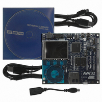
KIT DEV/EVAL FOR AVR32 AT32UC3A
Manufacturer
Atmel
Series
AVR®32r
Type
MCUr
Datasheets
1.ATAVRONE-PROBECBL.pdf
(16 pages)
2.ATEVK1104.pdf
(826 pages)
3.ATEVK1104.pdf
(90 pages)
4.ATEVK1104.pdf
(6 pages)
5.ATEVK1104.pdf
(12 pages)
Specifications of ATEVK1104
Contents
Evaluation Board, Software and Documentation
Processor To Be Evaluated
AT32UC3A3
Data Bus Width
32 bit
Interface Type
USB, SPI, USART
Silicon Manufacturer
Atmel
Core Architecture
AVR
Core Sub-architecture
AVR UC3
Silicon Core Number
AT32UC3A3256
Silicon Family Name
AVR
Kit Contents
Board CD Docs
Rohs Compliant
Yes
For Use With/related Products
AT32UC3A3
Lead Free Status / RoHS Status
Lead free / RoHS Compliant
Available stocks
Company
Part Number
Manufacturer
Quantity
Price
Company:

Part Number:
ATEVK1104
Manufacturer:
Atmel
Quantity:
135


35.4.1.3
35.4.1.4
35.4.1.5
35.4.2
35.4.2.1
35.4.2.2
35.4.3
32058J–AVR32–04/11
Memory Service Unit
AUX-based debug features
OCD Mode
Monitor Mode
Program Counter monitoring
Cyclic Redundancy Check (CRC)
NanoTrace
When a breakpoint triggers, the CPU enters OCD mode, and instructions are fetched from the
Debug Instruction OCD register. Each time this register is written by JTAG, the instruction is
executed, allowing the JTAG to execute CPU instructions directly. The JTAG master can e.g.
read out the register file by issuing mtdr instructions to the CPU, writing each register to the
Debug Communication Channel OCD registers.
Since the OCD registers are directly accessible by the CPU, it is possible to build a software-
based debugger that runs on the CPU itself. Setting the Monitor Mode bit in the Development
Control register causes the CPU to enter Monitor Mode instead of OCD mode when a breakpoint
triggers. Monitor Mode is similar to OCD mode, except that instructions are fetched from the
debug exception vector in regular program memory, instead of issued by JTAG.
Normally, the CPU would need to be halted for a JTAG-based debugger to examine the current
PC value. However, the AT32UC3A also proves a Debug Program Counter OCD register, where
the debugger can continuously read the current PC without affecting the CPU. This allows the
debugger to generate a simple statistic of the time spent in various areas of the code, easing
code optimization.
The Memory Service Unit (MSU) is a block dedicated to test and debug functionality. It is con-
trolled through a dedicated set of registers addressed through the MEMORY_SERVICE JTAG
command.
The MSU can be used to automatically calculate the CRC of a block of data in memory. The
OCD will then read out each word in the specified memory block and report the CRC32-value in
an OCD register.
The MSU additionally supports NanoTrace. This is an AVR32-specific feature, in which trace
data is output to memory instead of the AUX port. This allows the trace data to be extracted by
JTAG MEMORY_ACCESS, enabling trace features for JTAG-based debuggers. The user must
write MSU registers to configure the address and size of the memory block to be used for Nano-
Trace. The NanoTrace buffer can be anywhere in the physical address range, including internal
and external RAM, through an EBI, if present. This area may not be used by the application run-
ning on the CPU.
Utilizing the Auxiliary (AUX) port gives access to a wide range of advanced debug features. Of
prime importance are the trace features, which allow an external debugger to receive continuous
information on the program execution in the CPU. Additionally, Event In and Event Out pins
allow external events to be correlated with the program flow.
The AUX port contains a number of pins, as shown in
plexed with PIO lines, and must explicitly be enabled by writing OCD registers before the debug
session starts. The AUX port is mapped to two different locations, selectable by OCD Registers,
minimizing the chance that the AUX port will need to be shared with an application.
Table 35-1 on page
738. These are multi-
AT32UC3A
737
Related parts for ATEVK1104
Image
Part Number
Description
Manufacturer
Datasheet
Request
R

Part Number:
Description:
DEV KIT FOR AVR/AVR32
Manufacturer:
Atmel
Datasheet:

Part Number:
Description:
INTERVAL AND WIPE/WASH WIPER CONTROL IC WITH DELAY
Manufacturer:
ATMEL Corporation
Datasheet:
Part Number:
Description:
Low-Voltage Voice-Switched IC for Hands-Free Operation
Manufacturer:
ATMEL Corporation
Datasheet:
Part Number:
Description:
MONOLITHIC INTEGRATED FEATUREPHONE CIRCUIT
Manufacturer:
ATMEL Corporation
Datasheet:
Part Number:
Description:
AM-FM Receiver IC U4255BM-M
Manufacturer:
ATMEL Corporation
Datasheet:
Part Number:
Description:
Monolithic Integrated Feature Phone Circuit
Manufacturer:
ATMEL Corporation
Datasheet:
Part Number:
Description:
Multistandard Video-IF and Quasi Parallel Sound Processing
Manufacturer:
ATMEL Corporation
Datasheet:
Part Number:
Description:
High-performance EE PLD
Manufacturer:
ATMEL Corporation
Datasheet:
Part Number:
Description:
8-bit Flash Microcontroller
Manufacturer:
ATMEL Corporation
Datasheet:
Part Number:
Description:
2-Wire Serial EEPROM
Manufacturer:
ATMEL Corporation
Datasheet: